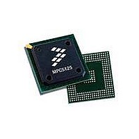
MPC5125YVN400 Freescale Semiconductor, MPC5125YVN400 Datasheet - Page 945

MPC5125YVN400
Manufacturer Part Number
MPC5125YVN400
Description
IC MCU 32BIT E300 324TEPBGA
Manufacturer
Freescale Semiconductor
Series
MPC51xxr
Datasheets
1.MPC5125YVN400.pdf
(92 pages)
2.MPC5125YVN400.pdf
(8 pages)
3.MPC5125YVN400.pdf
(2 pages)
4.MPC5125YVN400.pdf
(1064 pages)
Specifications of MPC5125YVN400
Core Processor
e300
Core Size
32-Bit
Speed
400MHz
Connectivity
CAN, EBI/EMI, Ethernet, I²C, USB OTG
Peripherals
DMA, WDT
Number Of I /o
64
Program Memory Type
ROMless
Ram Size
32K x 8
Voltage - Supply (vcc/vdd)
1.33 V ~ 1.47 V
Oscillator Type
External
Operating Temperature
-40°C ~ 125°C
Package / Case
324-PBGA
Processor Series
MPC51xx
Core
e300
Data Bus Width
32 bit
Development Tools By Supplier
TWR-MPC5125-KIT, TWR-SER, TWR-ELEV, TOWER
Maximum Clock Frequency
400 MHz
Operating Supply Voltage
1.4 V
Maximum Operating Temperature
+ 125 C
Mounting Style
SMD/SMT
Data Ram Size
32 KB
I/o Voltage
3.3 V
Interface Type
CAN, I2C
Minimum Operating Temperature
- 40 C
Program Memory Size
32 bit
Cpu Speed
400MHz
Embedded Interface Type
CAN, I2C, SPI, UART, USB
Digital Ic Case Style
TEPBGA
No. Of Pins
324
Rohs Compliant
Yes
Cpu Family
MPC5xx
Device Core Size
32b
Frequency (max)
400MHz
Total Internal Ram Size
32KB
Instruction Set Architecture
RISC
Operating Temp Range
-40C to 85C
Operating Temperature Classification
Industrial
Mounting
Surface Mount
Pin Count
324
Lead Free Status / RoHS Status
Lead free / RoHS Compliant
Eeprom Size
-
Program Memory Size
-
Data Converters
-
Lead Free Status / Rohs Status
Lead free / RoHS Compliant
Available stocks
Company
Part Number
Manufacturer
Quantity
Price
Company:
Part Number:
MPC5125YVN400
Manufacturer:
Freescale Semiconductor
Quantity:
135
Company:
Part Number:
MPC5125YVN400
Manufacturer:
LTC
Quantity:
29
Company:
Part Number:
MPC5125YVN400
Manufacturer:
Freescale Semiconductor
Quantity:
10 000
- MPC5125YVN400 PDF datasheet
- MPC5125YVN400 PDF datasheet #2
- MPC5125YVN400 PDF datasheet #3
- MPC5125YVN400 PDF datasheet #4
- Current page: 945 of 1064
- Download datasheet (6Mb)
The periodic frame list is effectively the leaf level a binary tree, which is always traversed leaf to root.
Each level in the tree corresponds to a 2
on the USB by spreading interrupt queue heads that have the same poll rate requirement across all the
available paths from the frame list. For example, system software can schedule eight poll rate eight queue
heads and account for them once in the high-speed bus bandwidth allocation.
When an endpoint is allocated an execution footprint that spans a frame boundary, the queue head for the
endpoint must be reachable from consecutive locations in the frame list. An example would be if 8
such an endpoint. Without additional support on the interface, to get 8
software would have to link 8
same path as 4
technique.
FSTN data structures are used to preserve the integrity of the binary-tree structure and enable the use of
the spreading technique.
hardware and software operational model requirements for using FSTNs.
The following queue head fields are initialized by system software to instruct the host controller when to
execute portions of the split-transaction protocol.
Freescale Semiconductor
•
•
Case 2a through Case 2c: The USB 2.0 hub pipeline rules states clearly, when and how many
complete-splits must be scheduled to account for earliest to latest execution on the full/low-speed
link. The complete-splits may span the H-Frame boundary when the start-split is in micro-frame 4
or later. When this occurs, the H-Frame to B-Frame alignment requires the queue head be reachable
from consecutive periodic frame list locations. System software cannot build an efficient schedule
that satisfies this requirement unless it uses FSTNs.
the periodic schedule.
SplitXState. This is a single bit residing in the status field of a queue head
is used to track the current state of the split transaction.
Figure 32-65. General Structure of EHCI Periodic Schedule Utilizing Interrupt Spreading
Frame List
0
. This upsets the integrity of the binary tree and disallows the use of the spreading
Periodic
Section 32.5.7, “Periodic Frame Span Traversal Node (FSTN),”
1
MPC5125 Microcontroller Reference Manual, Rev. 2
to 8
0b
•
•
•
. It would then have to move 4
N
poll rate. Software can efficiently manage periodic bandwidth
8
8
8
8
8
8
8
8
7
6
5
4
3
2
1
0
Level 8
8
0b
Linkage repeats every 8 for
remainder of frame list
Figure 32-65
Level 4
4
4
4
4
3
2
1
0
1
Universal Serial Bus Interface with On-The-Go
and everything linked after into the
Level 2
0b
2
2
reachable at the correct time,
1
0
illustrates the general layout of
1
Level 1
0
(Root)
(Table
• • •
32-59). This bit
defines the
0b
32-117
were
Related parts for MPC5125YVN400
Image
Part Number
Description
Manufacturer
Datasheet
Request
R
Part Number:
Description:
Mpc5125 Microcontroller Data Sheet
Manufacturer:
Freescale Semiconductor, Inc
Datasheet:

Part Number:
Description:
MPC5125 Microcontroller Data Sheet
Manufacturer:
FREESCALE [Freescale Semiconductor, Inc]
Datasheet:
Part Number:
Description:
Manufacturer:
Freescale Semiconductor, Inc
Datasheet:
Part Number:
Description:
Manufacturer:
Freescale Semiconductor, Inc
Datasheet:
Part Number:
Description:
Manufacturer:
Freescale Semiconductor, Inc
Datasheet:
Part Number:
Description:
Manufacturer:
Freescale Semiconductor, Inc
Datasheet:
Part Number:
Description:
Manufacturer:
Freescale Semiconductor, Inc
Datasheet:
Part Number:
Description:
Manufacturer:
Freescale Semiconductor, Inc
Datasheet:
Part Number:
Description:
Manufacturer:
Freescale Semiconductor, Inc
Datasheet:
Part Number:
Description:
Manufacturer:
Freescale Semiconductor, Inc
Datasheet:
Part Number:
Description:
Manufacturer:
Freescale Semiconductor, Inc
Datasheet:
Part Number:
Description:
Manufacturer:
Freescale Semiconductor, Inc
Datasheet:
Part Number:
Description:
Manufacturer:
Freescale Semiconductor, Inc
Datasheet:
Part Number:
Description:
Manufacturer:
Freescale Semiconductor, Inc
Datasheet:
Part Number:
Description:
Manufacturer:
Freescale Semiconductor, Inc
Datasheet:


