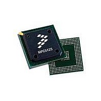
MPC5125YVN400 Freescale Semiconductor, MPC5125YVN400 Datasheet - Page 195

MPC5125YVN400
Manufacturer Part Number
MPC5125YVN400
Description
IC MCU 32BIT E300 324TEPBGA
Manufacturer
Freescale Semiconductor
Series
MPC51xxr
Datasheets
1.MPC5125YVN400.pdf
(92 pages)
2.MPC5125YVN400.pdf
(8 pages)
3.MPC5125YVN400.pdf
(2 pages)
4.MPC5125YVN400.pdf
(1064 pages)
Specifications of MPC5125YVN400
Core Processor
e300
Core Size
32-Bit
Speed
400MHz
Connectivity
CAN, EBI/EMI, Ethernet, I²C, USB OTG
Peripherals
DMA, WDT
Number Of I /o
64
Program Memory Type
ROMless
Ram Size
32K x 8
Voltage - Supply (vcc/vdd)
1.33 V ~ 1.47 V
Oscillator Type
External
Operating Temperature
-40°C ~ 125°C
Package / Case
324-PBGA
Processor Series
MPC51xx
Core
e300
Data Bus Width
32 bit
Development Tools By Supplier
TWR-MPC5125-KIT, TWR-SER, TWR-ELEV, TOWER
Maximum Clock Frequency
400 MHz
Operating Supply Voltage
1.4 V
Maximum Operating Temperature
+ 125 C
Mounting Style
SMD/SMT
Data Ram Size
32 KB
I/o Voltage
3.3 V
Interface Type
CAN, I2C
Minimum Operating Temperature
- 40 C
Program Memory Size
32 bit
Cpu Speed
400MHz
Embedded Interface Type
CAN, I2C, SPI, UART, USB
Digital Ic Case Style
TEPBGA
No. Of Pins
324
Rohs Compliant
Yes
Cpu Family
MPC5xx
Device Core Size
32b
Frequency (max)
400MHz
Total Internal Ram Size
32KB
Instruction Set Architecture
RISC
Operating Temp Range
-40C to 85C
Operating Temperature Classification
Industrial
Mounting
Surface Mount
Pin Count
324
Lead Free Status / RoHS Status
Lead free / RoHS Compliant
Eeprom Size
-
Program Memory Size
-
Data Converters
-
Lead Free Status / Rohs Status
Lead free / RoHS Compliant
Available stocks
Company
Part Number
Manufacturer
Quantity
Price
Company:
Part Number:
MPC5125YVN400
Manufacturer:
Freescale Semiconductor
Quantity:
135
Company:
Part Number:
MPC5125YVN400
Manufacturer:
LTC
Quantity:
29
Company:
Part Number:
MPC5125YVN400
Manufacturer:
Freescale Semiconductor
Quantity:
10 000
- MPC5125YVN400 PDF datasheet
- MPC5125YVN400 PDF datasheet #2
- MPC5125YVN400 PDF datasheet #3
- MPC5125YVN400 PDF datasheet #4
- Current page: 195 of 1064
- Download datasheet (6Mb)
6.4.9.2
In a diagnostic or production environment large amounts of data may need to be downloaded across the
network to a component or module. This data is often sent in a large block mode message (see above) that
violates the SAE J1850 limit for message length. To speed up the downloading of these large blocks of
data, they are sometimes transmitted at four times (4X) the normal bit rate for the Variable Pulse Width
modulation version of SAE J1850. This higher speed transmission, nominally 41.6 kbit/s, allows these
large blocks to be transmitted much more quickly.
The BDLC module is designed to receive and transmit messages at this higher speed. By setting the 4XE
bit in BDLC Control Register 2, the user can command the BDLC module to transmit and receive any
message over the network at a 4X rate.
If the BDLC module is placed in this 4X mode, messages transmitted at the normal bit rate are not received
correctly. Likewise, 4X messages transmitted on the SAE J1850 bus when the BDLC module is in normal
mode are interpreted as noise on the network by the BDLC module. For more information on the 4XE bit,
refer to
6.5
To initialize the BDLC module, the user should first write the desired data to the configuration bits. The
BDLC module should then be taken out of digital and analog loopback mode and enabled. Exiting from
loopback mode entails change of state indications in the BDLC_DLCBSVR register that must be dealt
with. After this is complete, CPU interrupts can be enabled (if desired), and then the BDLC module is
capable of SAE J1850 serial network communication. For an illustration of the sequence necessary for
initializing the BDLC module, refer to
6.5.1
The first step necessary for initializing the BDLC module following an MCU reset is to write the desired
values to each of the BDLC module control registers. This is best done by storing predetermined
initialization values directly into these registers. The following description outlines a basic flow for
initializing the BDLC module. This basic flow does not detail more elaborate initialization routines, such
as performing digital and analog loopback tests before enabling the BDLC module for SAE J1850
communication. However, from the following descriptions and the BDLC module specification, the user
should be able to develop routines for performing various diagnostic procedures such as loopback tests.
Freescale Semiconductor
1. Initialize the BDLC_DLCBARD register.
2. Initialize BDLC Baud Rate Select Register.
3. Initialize BDLC Control Register 2.
Begin initialization of the configuration bits by writing the desired analog transceiver
configuration data into the the BDLC_DLCBARD register. Following this write to the
BDLC_DLCBARD register, all of these bits become read only.
The next step in BDLC module initialization is to write the desired bus clock divisor minus one
into the BDLC Baud Rate Select Register. The divisor should be chosen to generate a 1 MHz or
1.048576 MHz MUX interface clock (f
Register, all of these bits become read only.
Section 6.4.4.1.5, “4X Mode.”
Initialization Information
Initializing the Configuration Bits
Transmitting Or Receiving A Message In 4X Mode
MPC5125 Microcontroller Reference Manual, Rev. 2
Figure
6-27.
bdlc
). Following this write to BDLC Baud Rate Select
Byte Data Link Controller (BDLC)
6-59
Related parts for MPC5125YVN400
Image
Part Number
Description
Manufacturer
Datasheet
Request
R
Part Number:
Description:
Mpc5125 Microcontroller Data Sheet
Manufacturer:
Freescale Semiconductor, Inc
Datasheet:

Part Number:
Description:
MPC5125 Microcontroller Data Sheet
Manufacturer:
FREESCALE [Freescale Semiconductor, Inc]
Datasheet:
Part Number:
Description:
Manufacturer:
Freescale Semiconductor, Inc
Datasheet:
Part Number:
Description:
Manufacturer:
Freescale Semiconductor, Inc
Datasheet:
Part Number:
Description:
Manufacturer:
Freescale Semiconductor, Inc
Datasheet:
Part Number:
Description:
Manufacturer:
Freescale Semiconductor, Inc
Datasheet:
Part Number:
Description:
Manufacturer:
Freescale Semiconductor, Inc
Datasheet:
Part Number:
Description:
Manufacturer:
Freescale Semiconductor, Inc
Datasheet:
Part Number:
Description:
Manufacturer:
Freescale Semiconductor, Inc
Datasheet:
Part Number:
Description:
Manufacturer:
Freescale Semiconductor, Inc
Datasheet:
Part Number:
Description:
Manufacturer:
Freescale Semiconductor, Inc
Datasheet:
Part Number:
Description:
Manufacturer:
Freescale Semiconductor, Inc
Datasheet:
Part Number:
Description:
Manufacturer:
Freescale Semiconductor, Inc
Datasheet:
Part Number:
Description:
Manufacturer:
Freescale Semiconductor, Inc
Datasheet:
Part Number:
Description:
Manufacturer:
Freescale Semiconductor, Inc
Datasheet:


