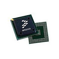
MPC5125YVN400 Freescale Semiconductor, MPC5125YVN400 Datasheet - Page 795

MPC5125YVN400
Manufacturer Part Number
MPC5125YVN400
Description
IC MCU 32BIT E300 324TEPBGA
Manufacturer
Freescale Semiconductor
Series
MPC51xxr
Datasheets
1.MPC5125YVN400.pdf
(92 pages)
2.MPC5125YVN400.pdf
(8 pages)
3.MPC5125YVN400.pdf
(2 pages)
4.MPC5125YVN400.pdf
(1064 pages)
Specifications of MPC5125YVN400
Core Processor
e300
Core Size
32-Bit
Speed
400MHz
Connectivity
CAN, EBI/EMI, Ethernet, I²C, USB OTG
Peripherals
DMA, WDT
Number Of I /o
64
Program Memory Type
ROMless
Ram Size
32K x 8
Voltage - Supply (vcc/vdd)
1.33 V ~ 1.47 V
Oscillator Type
External
Operating Temperature
-40°C ~ 125°C
Package / Case
324-PBGA
Processor Series
MPC51xx
Core
e300
Data Bus Width
32 bit
Development Tools By Supplier
TWR-MPC5125-KIT, TWR-SER, TWR-ELEV, TOWER
Maximum Clock Frequency
400 MHz
Operating Supply Voltage
1.4 V
Maximum Operating Temperature
+ 125 C
Mounting Style
SMD/SMT
Data Ram Size
32 KB
I/o Voltage
3.3 V
Interface Type
CAN, I2C
Minimum Operating Temperature
- 40 C
Program Memory Size
32 bit
Cpu Speed
400MHz
Embedded Interface Type
CAN, I2C, SPI, UART, USB
Digital Ic Case Style
TEPBGA
No. Of Pins
324
Rohs Compliant
Yes
Cpu Family
MPC5xx
Device Core Size
32b
Frequency (max)
400MHz
Total Internal Ram Size
32KB
Instruction Set Architecture
RISC
Operating Temp Range
-40C to 85C
Operating Temperature Classification
Industrial
Mounting
Surface Mount
Pin Count
324
Lead Free Status / RoHS Status
Lead free / RoHS Compliant
Eeprom Size
-
Program Memory Size
-
Data Converters
-
Lead Free Status / Rohs Status
Lead free / RoHS Compliant
Available stocks
Company
Part Number
Manufacturer
Quantity
Price
Company:
Part Number:
MPC5125YVN400
Manufacturer:
Freescale Semiconductor
Quantity:
135
Company:
Part Number:
MPC5125YVN400
Manufacturer:
LTC
Quantity:
29
Company:
Part Number:
MPC5125YVN400
Manufacturer:
Freescale Semiconductor
Quantity:
10 000
- MPC5125YVN400 PDF datasheet
- MPC5125YVN400 PDF datasheet #2
- MPC5125YVN400 PDF datasheet #3
- MPC5125YVN400 PDF datasheet #4
- Current page: 795 of 1064
- Download datasheet (6Mb)
28.4
The SDHC module controls the MMC, SD memory card, and I/O cards by sending commands to cards and
performing data accesses to/from the cards.
The following sections provide a brief functional description of the major system blocks, including the
DMA interface, memory controller, logic/command controller, and system clock controller.
28.4.1
The SDHC uses two data buffers in an alternating manner to transfer data through the DMA and the SD
card simultaneously to maximize throughput between the two clock domains (the IP peripheral clock,
IPG_PERCLCK, and the host clock, CLK_20M). See
scheme. These buffers are used as temporary storage for data transferred between the host system and the
card.
Freescale Semiconductor
FIFO CONTENT FIFO Content. These bits hold 32-bit data upon a read or write transfer. The size of the FIFO is 4 × 32 bits
Address: Base + 0x38
Reset
Reset
Field
W
W
R
R
Functional Description
16
0
0
0
Data Buffers
Figure 28-15. SDHC Data Buffer Access (SDHC_BUFFER_ACCESS) Register
(16 bytes in total) for SD 1-bit mode and 16 × 32 bits (64 bytes in total) for SD 4-bit mode. For reception, the
SDHC controller generates a DMA request when the FIFO is full. Upon receiving this request, the DMA starts
transferring data from the SDHC FIFO to system memory by reading the data buffer access register for a
number of pre-defined bytes. For transmit, the SDHC controller generates a DMA request when the FIFO is
empty. Upon receiving this request, the DMA starts moving data from the system memory to the SDHC FIFO
by writing to the data buffer access register for a number of pre-defined bytes.
17
0
0
1
18
0
0
2
Table 28-18. SDHC_BUFFER_ACCESS field descriptions
19
0
0
3
MPC5125 Microcontroller Reference Manual, Rev. 2
20
4
0
0
21
0
0
5
22
FIFO CONTENT[16:31]
0
0
6
FIFO CONTENT[0:15]
23
0
0
7
Figure 28-16
Description
24
8
0
0
25
9
0
0
for illustration of the buffering
10
26
0
0
Secure Digital Host Controller (SDHC)
11
27
0
0
12
28
0
0
Access: User read/write
13
29
0
0
14
30
0
0
28-23
15
31
0
0
Related parts for MPC5125YVN400
Image
Part Number
Description
Manufacturer
Datasheet
Request
R
Part Number:
Description:
Mpc5125 Microcontroller Data Sheet
Manufacturer:
Freescale Semiconductor, Inc
Datasheet:

Part Number:
Description:
MPC5125 Microcontroller Data Sheet
Manufacturer:
FREESCALE [Freescale Semiconductor, Inc]
Datasheet:
Part Number:
Description:
Manufacturer:
Freescale Semiconductor, Inc
Datasheet:
Part Number:
Description:
Manufacturer:
Freescale Semiconductor, Inc
Datasheet:
Part Number:
Description:
Manufacturer:
Freescale Semiconductor, Inc
Datasheet:
Part Number:
Description:
Manufacturer:
Freescale Semiconductor, Inc
Datasheet:
Part Number:
Description:
Manufacturer:
Freescale Semiconductor, Inc
Datasheet:
Part Number:
Description:
Manufacturer:
Freescale Semiconductor, Inc
Datasheet:
Part Number:
Description:
Manufacturer:
Freescale Semiconductor, Inc
Datasheet:
Part Number:
Description:
Manufacturer:
Freescale Semiconductor, Inc
Datasheet:
Part Number:
Description:
Manufacturer:
Freescale Semiconductor, Inc
Datasheet:
Part Number:
Description:
Manufacturer:
Freescale Semiconductor, Inc
Datasheet:
Part Number:
Description:
Manufacturer:
Freescale Semiconductor, Inc
Datasheet:
Part Number:
Description:
Manufacturer:
Freescale Semiconductor, Inc
Datasheet:
Part Number:
Description:
Manufacturer:
Freescale Semiconductor, Inc
Datasheet:


