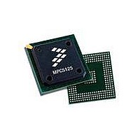
MPC5125YVN400 Freescale Semiconductor, MPC5125YVN400 Datasheet - Page 658

MPC5125YVN400
Manufacturer Part Number
MPC5125YVN400
Description
IC MCU 32BIT E300 324TEPBGA
Manufacturer
Freescale Semiconductor
Series
MPC51xxr
Datasheets
1.MPC5125YVN400.pdf
(92 pages)
2.MPC5125YVN400.pdf
(8 pages)
3.MPC5125YVN400.pdf
(2 pages)
4.MPC5125YVN400.pdf
(1064 pages)
Specifications of MPC5125YVN400
Core Processor
e300
Core Size
32-Bit
Speed
400MHz
Connectivity
CAN, EBI/EMI, Ethernet, I²C, USB OTG
Peripherals
DMA, WDT
Number Of I /o
64
Program Memory Type
ROMless
Ram Size
32K x 8
Voltage - Supply (vcc/vdd)
1.33 V ~ 1.47 V
Oscillator Type
External
Operating Temperature
-40°C ~ 125°C
Package / Case
324-PBGA
Processor Series
MPC51xx
Core
e300
Data Bus Width
32 bit
Development Tools By Supplier
TWR-MPC5125-KIT, TWR-SER, TWR-ELEV, TOWER
Maximum Clock Frequency
400 MHz
Operating Supply Voltage
1.4 V
Maximum Operating Temperature
+ 125 C
Mounting Style
SMD/SMT
Data Ram Size
32 KB
I/o Voltage
3.3 V
Interface Type
CAN, I2C
Minimum Operating Temperature
- 40 C
Program Memory Size
32 bit
Cpu Speed
400MHz
Embedded Interface Type
CAN, I2C, SPI, UART, USB
Digital Ic Case Style
TEPBGA
No. Of Pins
324
Rohs Compliant
Yes
Cpu Family
MPC5xx
Device Core Size
32b
Frequency (max)
400MHz
Total Internal Ram Size
32KB
Instruction Set Architecture
RISC
Operating Temp Range
-40C to 85C
Operating Temperature Classification
Industrial
Mounting
Surface Mount
Pin Count
324
Lead Free Status / RoHS Status
Lead free / RoHS Compliant
Eeprom Size
-
Program Memory Size
-
Data Converters
-
Lead Free Status / Rohs Status
Lead free / RoHS Compliant
Available stocks
Company
Part Number
Manufacturer
Quantity
Price
Company:
Part Number:
MPC5125YVN400
Manufacturer:
Freescale Semiconductor
Quantity:
135
Company:
Part Number:
MPC5125YVN400
Manufacturer:
LTC
Quantity:
29
Company:
Part Number:
MPC5125YVN400
Manufacturer:
Freescale Semiconductor
Quantity:
10 000
- MPC5125YVN400 PDF datasheet
- MPC5125YVN400 PDF datasheet #2
- MPC5125YVN400 PDF datasheet #3
- MPC5125YVN400 PDF datasheet #4
- Current page: 658 of 1064
- Download datasheet (6Mb)
NAND Flash Controller (NFC)
Boot-up occurs after power-on reset. After boot, the following happens.
The boot is identical for a 8-wide and 16-wide flash. If a 16-wide flash is connected, the data on the upper
lane are discarded. If a 8-wide flash is connected, the upper 1 KB of data are not read. See
23-28
Suppose the boot code is U0,U1,U2,U3,... each of them is an 8-byte data (U0=byte0-7,U1=byte8-15,...), flash device data
width is 8-bit. Data organization in the NAND Flash is page0:U0,U4,U8,U12,...; page1:U1,U5,U9,U13,...;
page2:U2,U6,U10,U14,...; page3:U3,U7,U11,U14,...
•
•
•
1. 4 boot blocks are identified in the flash. These are blocks at row address 0, 256, 512, and 768.
2. The flash controller does a burst read from the first boot block to memory.The burst is 4 pages long,
3. If no ECC failure occurs during the burst read, boot is successful.
4. If an ECC failure occurs during the burst read, the process is started again from the next boot block.
5. CPU access is held until boot completion.
6. After boot, boot image is visible on IPS memory map, address 0 to 3983. A special hash function
Physical
0x00-1F
0x20-3F
0x40-5F
0x60-7F
Page
Flash is defined as 8-bit: 16BIT = 0
ECC correction depth is 32 bits errors: ECC_MODE = 0b111
Boot sector address is 0: BUFNO = 0b00
so a total of 4 KB are read in this way.
If the fourth block still has an ECC failure, the boot is unsuccessful, , which means it is not possible
to read a reliable boot image from the flash.
is active on the NFC SRAM read to have the boot image in one continuous address range, and not
in 4 address ranges, one for each page. The config bit BOOT_MODE controls this hash function,
and this bit should be turned off after the CPU has read/executed the boot image, and before it
operates the NFC in the standard mode. See
Addr
......
Buffer
U0
U4
U8
U12
...
U0
U4
U8
U12
...
0
0
U1
U5
U9
U13
...
U1
U5
U9
U13
...
1
1
U2
U6
U10
U14
...
U2
U6
U10
U14
...
read 4 pages, each
page 1056 bytes
2
2
MPC5125 Microcontroller Reference Manual, Rev. 2
U3
U7
U11
U15
...
U3
U7
U11
U15
...
3
3
Figure 23-25. Boot and BOOT_MODE
When boot starts, BOOT_MODE is set to 1. After boot_done,
if CPU reads data from the 0x0000 of SRAM buffer, the data is
U0,U1,U2,U3,U4,U5,U6,U7,......
If BOOT_MODE is set to 0 (non-boot mode), CPU will read
U0,U4,U8,U12,... from address 0x0000(buffer0),
U1,U5,U9,U13,... from address 0x1000(buffer1),
U2,U6,U10,U14,... from address 0x2000(buffer2),
U3,U7,U11,U15,... from address 0x3000(buffer3).
Because there’s no difference in the way that data being
transferred between SRAM buffer and the flash: one page
uses one buffer. But the way CPU writes/reads buffer is
different. In non-boot mode, there’s a transition between CPU
and SRAM physical address, see
Memory
Figure
Space”
23-25.
Section 23.5, “NFC Buffer
Freescale Semiconductor
Figure
23-26.
Related parts for MPC5125YVN400
Image
Part Number
Description
Manufacturer
Datasheet
Request
R
Part Number:
Description:
Mpc5125 Microcontroller Data Sheet
Manufacturer:
Freescale Semiconductor, Inc
Datasheet:

Part Number:
Description:
MPC5125 Microcontroller Data Sheet
Manufacturer:
FREESCALE [Freescale Semiconductor, Inc]
Datasheet:
Part Number:
Description:
Manufacturer:
Freescale Semiconductor, Inc
Datasheet:
Part Number:
Description:
Manufacturer:
Freescale Semiconductor, Inc
Datasheet:
Part Number:
Description:
Manufacturer:
Freescale Semiconductor, Inc
Datasheet:
Part Number:
Description:
Manufacturer:
Freescale Semiconductor, Inc
Datasheet:
Part Number:
Description:
Manufacturer:
Freescale Semiconductor, Inc
Datasheet:
Part Number:
Description:
Manufacturer:
Freescale Semiconductor, Inc
Datasheet:
Part Number:
Description:
Manufacturer:
Freescale Semiconductor, Inc
Datasheet:
Part Number:
Description:
Manufacturer:
Freescale Semiconductor, Inc
Datasheet:
Part Number:
Description:
Manufacturer:
Freescale Semiconductor, Inc
Datasheet:
Part Number:
Description:
Manufacturer:
Freescale Semiconductor, Inc
Datasheet:
Part Number:
Description:
Manufacturer:
Freescale Semiconductor, Inc
Datasheet:
Part Number:
Description:
Manufacturer:
Freescale Semiconductor, Inc
Datasheet:
Part Number:
Description:
Manufacturer:
Freescale Semiconductor, Inc
Datasheet:


