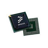
MPC5125YVN400 Freescale Semiconductor, MPC5125YVN400 Datasheet - Page 802

MPC5125YVN400
Manufacturer Part Number
MPC5125YVN400
Description
IC MCU 32BIT E300 324TEPBGA
Manufacturer
Freescale Semiconductor
Series
MPC51xxr
Datasheets
1.MPC5125YVN400.pdf
(92 pages)
2.MPC5125YVN400.pdf
(8 pages)
3.MPC5125YVN400.pdf
(2 pages)
4.MPC5125YVN400.pdf
(1064 pages)
Specifications of MPC5125YVN400
Core Processor
e300
Core Size
32-Bit
Speed
400MHz
Connectivity
CAN, EBI/EMI, Ethernet, I²C, USB OTG
Peripherals
DMA, WDT
Number Of I /o
64
Program Memory Type
ROMless
Ram Size
32K x 8
Voltage - Supply (vcc/vdd)
1.33 V ~ 1.47 V
Oscillator Type
External
Operating Temperature
-40°C ~ 125°C
Package / Case
324-PBGA
Processor Series
MPC51xx
Core
e300
Data Bus Width
32 bit
Development Tools By Supplier
TWR-MPC5125-KIT, TWR-SER, TWR-ELEV, TOWER
Maximum Clock Frequency
400 MHz
Operating Supply Voltage
1.4 V
Maximum Operating Temperature
+ 125 C
Mounting Style
SMD/SMT
Data Ram Size
32 KB
I/o Voltage
3.3 V
Interface Type
CAN, I2C
Minimum Operating Temperature
- 40 C
Program Memory Size
32 bit
Cpu Speed
400MHz
Embedded Interface Type
CAN, I2C, SPI, UART, USB
Digital Ic Case Style
TEPBGA
No. Of Pins
324
Rohs Compliant
Yes
Cpu Family
MPC5xx
Device Core Size
32b
Frequency (max)
400MHz
Total Internal Ram Size
32KB
Instruction Set Architecture
RISC
Operating Temp Range
-40C to 85C
Operating Temperature Classification
Industrial
Mounting
Surface Mount
Pin Count
324
Lead Free Status / RoHS Status
Lead free / RoHS Compliant
Eeprom Size
-
Program Memory Size
-
Data Converters
-
Lead Free Status / Rohs Status
Lead free / RoHS Compliant
Available stocks
Company
Part Number
Manufacturer
Quantity
Price
Company:
Part Number:
MPC5125YVN400
Manufacturer:
Freescale Semiconductor
Quantity:
135
Company:
Part Number:
MPC5125YVN400
Manufacturer:
LTC
Quantity:
29
Company:
Part Number:
MPC5125YVN400
Manufacturer:
Freescale Semiconductor
Quantity:
10 000
- MPC5125YVN400 PDF datasheet
- MPC5125YVN400 PDF datasheet #2
- MPC5125YVN400 PDF datasheet #3
- MPC5125YVN400 PDF datasheet #4
- Current page: 802 of 1064
- Download datasheet (6Mb)
Secure Digital Host Controller (SDHC)
For multiple block data transfers in 4-bit mode, the interrupt period can be active for only a limited period
of time, due to the limited period of data line availability between multiple blocks of data. This requires a
more strict definition of the interrupt period. For this case, the interrupt period is limited to two
MMC_SD_CLK clock cycles. This begins two clocks after the end bit of the previous data block. During
this 2-clock cycle interrupt period, if an interrupt is pending, the DAT1 line is held low for one clock cycle
with the last clock cycle pulling DAT1 high. On completion of the interrupt period, the card releases the
DAT1 line into the high impedance state.
When in 4-bit mode, the SDHC differentiates a data start bit and the interrupt period by checking all four
data lines are low for the start of new data. In the case of an interrupt, only the DAT1 should have gone
low. After the last data block is sent, the interrupt period starts as normal after the end of this data block,
but it ends after the next command with a data block commences, instead of lasting two cycles.
Refer to the SDIO Card Specification for further information about the SDIO card interrupt.
28.4.4.3
Card Interrupt Handling
When the SDIO_IRQ_EN bit in the SDHC Interrupt Control register (SDHC_INT_CNTR) is set to 0, the
host controller clears the interrupt request to the system interrupt controller. The SDIO Interrupt detection
is stopped when this bit is cleared and restarted when this bit is set to 1. The host driver should clear the
SDIO interrupt enable bit before servicing the SDIO interrupt and should set this bit again after all interrupt
requests from the card are cleared to prevent inadvertent interrupts.
The SDIO Status bit is cleared by resetting the SDIO interrupt. Writing to this bit has effect in 1-bit mode,
as the host controller detects the SDIO interrupt with or without SD clock (to support wakeup). In 4-bit
mode, the interrupt signal is sampled during the interrupt period; therefore, some sample delays exist
between the interrupt signal from the SDIO card and the interrupt to the host system interrupt controller.
When the SDIO status has been set and the host driver needs to start this interrupt service, the SDIO bit in
the interrupt control register is set to 0 to clear the SDIO interrupt status latched in the SDHC and to stop
driving the interrupt signal to the system interrupt controller. The host driver must issue a CMD52 to clear
the interrupts at the card. After completion of the card interrupt service, the SDIO interrupt enable bit is
set to 1 and SDHC starts sampling the interrupt signal again. See
Figure 28-21
(a) for illustration of the
SDIO card interrupt scheme and
Figure 28-21
(b) for the sequences of software and hardware events
taking place during card interrupt handling procedure
MPC5125 Microcontroller Reference Manual, Rev. 2
28-30
Freescale Semiconductor
Related parts for MPC5125YVN400
Image
Part Number
Description
Manufacturer
Datasheet
Request
R
Part Number:
Description:
Mpc5125 Microcontroller Data Sheet
Manufacturer:
Freescale Semiconductor, Inc
Datasheet:

Part Number:
Description:
MPC5125 Microcontroller Data Sheet
Manufacturer:
FREESCALE [Freescale Semiconductor, Inc]
Datasheet:
Part Number:
Description:
Manufacturer:
Freescale Semiconductor, Inc
Datasheet:
Part Number:
Description:
Manufacturer:
Freescale Semiconductor, Inc
Datasheet:
Part Number:
Description:
Manufacturer:
Freescale Semiconductor, Inc
Datasheet:
Part Number:
Description:
Manufacturer:
Freescale Semiconductor, Inc
Datasheet:
Part Number:
Description:
Manufacturer:
Freescale Semiconductor, Inc
Datasheet:
Part Number:
Description:
Manufacturer:
Freescale Semiconductor, Inc
Datasheet:
Part Number:
Description:
Manufacturer:
Freescale Semiconductor, Inc
Datasheet:
Part Number:
Description:
Manufacturer:
Freescale Semiconductor, Inc
Datasheet:
Part Number:
Description:
Manufacturer:
Freescale Semiconductor, Inc
Datasheet:
Part Number:
Description:
Manufacturer:
Freescale Semiconductor, Inc
Datasheet:
Part Number:
Description:
Manufacturer:
Freescale Semiconductor, Inc
Datasheet:
Part Number:
Description:
Manufacturer:
Freescale Semiconductor, Inc
Datasheet:
Part Number:
Description:
Manufacturer:
Freescale Semiconductor, Inc
Datasheet:


