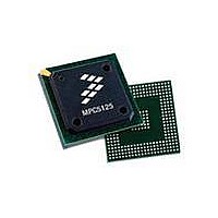
MPC5125YVN400 Freescale Semiconductor, MPC5125YVN400 Datasheet - Page 603

MPC5125YVN400
Manufacturer Part Number
MPC5125YVN400
Description
IC MCU 32BIT E300 324TEPBGA
Manufacturer
Freescale Semiconductor
Series
MPC51xxr
Datasheets
1.MPC5125YVN400.pdf
(92 pages)
2.MPC5125YVN400.pdf
(8 pages)
3.MPC5125YVN400.pdf
(2 pages)
4.MPC5125YVN400.pdf
(1064 pages)
Specifications of MPC5125YVN400
Core Processor
e300
Core Size
32-Bit
Speed
400MHz
Connectivity
CAN, EBI/EMI, Ethernet, I²C, USB OTG
Peripherals
DMA, WDT
Number Of I /o
64
Program Memory Type
ROMless
Ram Size
32K x 8
Voltage - Supply (vcc/vdd)
1.33 V ~ 1.47 V
Oscillator Type
External
Operating Temperature
-40°C ~ 125°C
Package / Case
324-PBGA
Processor Series
MPC51xx
Core
e300
Data Bus Width
32 bit
Development Tools By Supplier
TWR-MPC5125-KIT, TWR-SER, TWR-ELEV, TOWER
Maximum Clock Frequency
400 MHz
Operating Supply Voltage
1.4 V
Maximum Operating Temperature
+ 125 C
Mounting Style
SMD/SMT
Data Ram Size
32 KB
I/o Voltage
3.3 V
Interface Type
CAN, I2C
Minimum Operating Temperature
- 40 C
Program Memory Size
32 bit
Cpu Speed
400MHz
Embedded Interface Type
CAN, I2C, SPI, UART, USB
Digital Ic Case Style
TEPBGA
No. Of Pins
324
Rohs Compliant
Yes
Cpu Family
MPC5xx
Device Core Size
32b
Frequency (max)
400MHz
Total Internal Ram Size
32KB
Instruction Set Architecture
RISC
Operating Temp Range
-40C to 85C
Operating Temperature Classification
Industrial
Mounting
Surface Mount
Pin Count
324
Lead Free Status / RoHS Status
Lead free / RoHS Compliant
Eeprom Size
-
Program Memory Size
-
Data Converters
-
Lead Free Status / Rohs Status
Lead free / RoHS Compliant
Available stocks
Company
Part Number
Manufacturer
Quantity
Price
Company:
Part Number:
MPC5125YVN400
Manufacturer:
Freescale Semiconductor
Quantity:
135
Company:
Part Number:
MPC5125YVN400
Manufacturer:
LTC
Quantity:
29
Company:
Part Number:
MPC5125YVN400
Manufacturer:
Freescale Semiconductor
Quantity:
10 000
- MPC5125YVN400 PDF datasheet
- MPC5125YVN400 PDF datasheet #2
- MPC5125YVN400 PDF datasheet #3
- MPC5125YVN400 PDF datasheet #4
- Current page: 603 of 1064
- Download datasheet (6Mb)
The acceptance registers of the MSCAN are applied on the IDR0–IDR3 registers (see
“Identifier Registers
“Identifier Acceptance
For extended identifiers, all four acceptance and mask registers are applied. For standard identifiers, only
the first two (CANIDAR0/1, CANIDMR0/1) are applied.
22.3.2.17 MSCAN Identifier Mask Register (CANIDMR0–CANIDMR7)
The identifier mask register specifies which of the corresponding bits in the identifier acceptance register
are relevant for acceptance filtering.
22.3.3
The following section details the organization of the receive and transmit message buffers and the
associated control registers.
Freescale Semiconductor
Address: Base + 0x28 (CANIDMR0)
•
•
AM[7:0]
Reset
Field
To receive standard identifiers in 32-bit filter mode, the last three bits (AM[0:2]) in the following
mask registers must be programmed as “don’t care:”
— CANIDMR1
— CANIDMR5
To receive standard identifiers in 16-bit filter mode, the last three bits (AM[0:2]) in the following
mask registers must be programmed as “don’t care:”
— CANIDMR1
— CANIDMR3
— CANIDMR5
— CANIDMR7
W
R
Base + 0x29 (CANIDMR1)
Base + 0x24 (CANIDMRC)
Base + 0x25 (CANIDMRD)
Programmer’s Model of Message Storage
AM7
Acceptance Mask Bits. If a particular bit in this register is cleared, this indicates the corresponding bit in the
identifier acceptance register must be the same as its identifier bit before a match is detected. The message
is accepted if all such bits match. If a bit is set, it indicates the state of the corresponding bit in the identifier
acceptance register does not affect whether or not message is accepted.
0 Match corresponding acceptance code register and identifier bits.
1 Ignore corresponding acceptance code register bit.
0
0
Figure 22-19. MSCAN Identifier Mask Registers (CANIDMR0–CANIDMR7)
(IDR0–IDR3)”) of incoming messages in a bit-by-bit manner (see
Filter”).
Table 22-20. CANIDMR0–CANIDMR7 field descriptions
AM6
1
0
MPC5125 Microcontroller Reference Manual, Rev. 2
AM5
0
2
Base + 0x38 (CANIDMR4)
Base + 0x39 (CANIDMR5)
Base + 0x3C (CANIDMR6)
Base + 0x3D (CANIDMR7)
AM4
0
3
Description
AM3
0
4
AM2
0
5
Access: User read/write
AM1
Section 22.3.3.1,
0
6
Section 22.4.3,
AM0
0
7
MSCAN
22-25
Related parts for MPC5125YVN400
Image
Part Number
Description
Manufacturer
Datasheet
Request
R
Part Number:
Description:
Mpc5125 Microcontroller Data Sheet
Manufacturer:
Freescale Semiconductor, Inc
Datasheet:

Part Number:
Description:
MPC5125 Microcontroller Data Sheet
Manufacturer:
FREESCALE [Freescale Semiconductor, Inc]
Datasheet:
Part Number:
Description:
Manufacturer:
Freescale Semiconductor, Inc
Datasheet:
Part Number:
Description:
Manufacturer:
Freescale Semiconductor, Inc
Datasheet:
Part Number:
Description:
Manufacturer:
Freescale Semiconductor, Inc
Datasheet:
Part Number:
Description:
Manufacturer:
Freescale Semiconductor, Inc
Datasheet:
Part Number:
Description:
Manufacturer:
Freescale Semiconductor, Inc
Datasheet:
Part Number:
Description:
Manufacturer:
Freescale Semiconductor, Inc
Datasheet:
Part Number:
Description:
Manufacturer:
Freescale Semiconductor, Inc
Datasheet:
Part Number:
Description:
Manufacturer:
Freescale Semiconductor, Inc
Datasheet:
Part Number:
Description:
Manufacturer:
Freescale Semiconductor, Inc
Datasheet:
Part Number:
Description:
Manufacturer:
Freescale Semiconductor, Inc
Datasheet:
Part Number:
Description:
Manufacturer:
Freescale Semiconductor, Inc
Datasheet:
Part Number:
Description:
Manufacturer:
Freescale Semiconductor, Inc
Datasheet:
Part Number:
Description:
Manufacturer:
Freescale Semiconductor, Inc
Datasheet:


