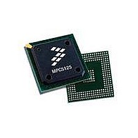
MPC5125YVN400 Freescale Semiconductor, MPC5125YVN400 Datasheet - Page 862

MPC5125YVN400
Manufacturer Part Number
MPC5125YVN400
Description
IC MCU 32BIT E300 324TEPBGA
Manufacturer
Freescale Semiconductor
Series
MPC51xxr
Datasheets
1.MPC5125YVN400.pdf
(92 pages)
2.MPC5125YVN400.pdf
(8 pages)
3.MPC5125YVN400.pdf
(2 pages)
4.MPC5125YVN400.pdf
(1064 pages)
Specifications of MPC5125YVN400
Core Processor
e300
Core Size
32-Bit
Speed
400MHz
Connectivity
CAN, EBI/EMI, Ethernet, I²C, USB OTG
Peripherals
DMA, WDT
Number Of I /o
64
Program Memory Type
ROMless
Ram Size
32K x 8
Voltage - Supply (vcc/vdd)
1.33 V ~ 1.47 V
Oscillator Type
External
Operating Temperature
-40°C ~ 125°C
Package / Case
324-PBGA
Processor Series
MPC51xx
Core
e300
Data Bus Width
32 bit
Development Tools By Supplier
TWR-MPC5125-KIT, TWR-SER, TWR-ELEV, TOWER
Maximum Clock Frequency
400 MHz
Operating Supply Voltage
1.4 V
Maximum Operating Temperature
+ 125 C
Mounting Style
SMD/SMT
Data Ram Size
32 KB
I/o Voltage
3.3 V
Interface Type
CAN, I2C
Minimum Operating Temperature
- 40 C
Program Memory Size
32 bit
Cpu Speed
400MHz
Embedded Interface Type
CAN, I2C, SPI, UART, USB
Digital Ic Case Style
TEPBGA
No. Of Pins
324
Rohs Compliant
Yes
Cpu Family
MPC5xx
Device Core Size
32b
Frequency (max)
400MHz
Total Internal Ram Size
32KB
Instruction Set Architecture
RISC
Operating Temp Range
-40C to 85C
Operating Temperature Classification
Industrial
Mounting
Surface Mount
Pin Count
324
Lead Free Status / RoHS Status
Lead free / RoHS Compliant
Eeprom Size
-
Program Memory Size
-
Data Converters
-
Lead Free Status / Rohs Status
Lead free / RoHS Compliant
Available stocks
Company
Part Number
Manufacturer
Quantity
Price
Company:
Part Number:
MPC5125YVN400
Manufacturer:
Freescale Semiconductor
Quantity:
135
Company:
Part Number:
MPC5125YVN400
Manufacturer:
LTC
Quantity:
29
Company:
Part Number:
MPC5125YVN400
Manufacturer:
Freescale Semiconductor
Quantity:
10 000
- MPC5125YVN400 PDF datasheet
- MPC5125YVN400 PDF datasheet #2
- MPC5125YVN400 PDF datasheet #3
- MPC5125YVN400 PDF datasheet #4
- Current page: 862 of 1064
- Download datasheet (6Mb)
Universal Serial Bus Interface with On-The-Go
Two operations, wake-up and read/write, can be performed with the ULPI Viewport. Wake-up operation
puts the ULPI interface into normal operation mode and re-enables the clock if necessary. A wakeup
operation is required before accessing the registers when ULPI interface is operating in low-power mode,
serial mode, or carkit mode. The ULPI state can be determined by reading the sync. state bit (ULPISS). If
this bit is a 1, ULPI interface is running in normal operation mode and can accept read/write operations.
If the ULPISS indicates a 0, read/write operations are not able to execute. Undefined behavior results if
ULPISS equals 0 and a read or write operation is performed. To execute a wakeup operation, write all 32
bits of the ULPI Viewport where ULPIPORT is constructed appropriately and the ULPIWU bit is 1 and
ULPIRUN bit is 0. Poll the ULPI viewport until ULPIWU is 0 for the operation to complete.
To execute a read or write operation, write all 32 bits of the ULPI Viewport where ULPIDATWR,
ULPIADDR, ULPIPORT, and ULPIRW are constructed appropriately and the ULPIRUN bit is 1. Poll the
ULPI Viewport until ULPIRUN is 0 for the operation to complete. After ULPIRUN is 0, ULPIDATRD is
valid if the operation was a read.
The polling method above could also be replaced by an interrupt driven routine using the ULPI interrupt
defined in the USB_USBSTS and USB_USBINTR registers. When a wakeup or read/write operation
complete, the ULPI interrupt is set.
There are several optional features that system software may need to enable or disable as part of system
configuration. These bits are contained in the interface and OTG control registers of the ULPI PHY
register set. These registers also contain bits controlled by the link dynamically and therefore should only
be modified by system software using the set/clear access method. Direct writes to these registers could
have harmful side effects to the standard USB operations. The optional bits are as follows: bits 3 through
7 in the interface control register and bits 6 and 7 in the OTG control register. Refer to the ULPI
Specification Revision 1.1 for further information on the use of the optional features.
32-34
Address: Base + 0x170
Reset
Reset
W
W
R
R
ULPI
WU
16
0
0
0
Writes to the ULPI through the viewport can substantially harm standard
USB operations. Read operations should have no harmful side effects to
standard USB operations.
ULPI
RUN
17
0
0
1
ULPI
RW
Figure 32-27. ULPI Viewport (USB_ULPIVIEWPORT) Register
18
0
0
2
ULPIDARD
19
R
0
0
3
MPC5125 Microcontroller Reference Manual, Rev. 2
ULPI
SS
20
4
1
0
21
0
0
5
ULPIPORT
CAUTION
22
0
0
6
23
0
0
7
24
8
0
0
25
9
0
0
10
26
0
0
ULPIDATWR
ULPIADDR
11
27
0
0
12
28
0
0
Freescale Semiconductor
Access: User read/write
13
29
0
0
14
30
0
0
15
31
0
0
Related parts for MPC5125YVN400
Image
Part Number
Description
Manufacturer
Datasheet
Request
R
Part Number:
Description:
Mpc5125 Microcontroller Data Sheet
Manufacturer:
Freescale Semiconductor, Inc
Datasheet:

Part Number:
Description:
MPC5125 Microcontroller Data Sheet
Manufacturer:
FREESCALE [Freescale Semiconductor, Inc]
Datasheet:
Part Number:
Description:
Manufacturer:
Freescale Semiconductor, Inc
Datasheet:
Part Number:
Description:
Manufacturer:
Freescale Semiconductor, Inc
Datasheet:
Part Number:
Description:
Manufacturer:
Freescale Semiconductor, Inc
Datasheet:
Part Number:
Description:
Manufacturer:
Freescale Semiconductor, Inc
Datasheet:
Part Number:
Description:
Manufacturer:
Freescale Semiconductor, Inc
Datasheet:
Part Number:
Description:
Manufacturer:
Freescale Semiconductor, Inc
Datasheet:
Part Number:
Description:
Manufacturer:
Freescale Semiconductor, Inc
Datasheet:
Part Number:
Description:
Manufacturer:
Freescale Semiconductor, Inc
Datasheet:
Part Number:
Description:
Manufacturer:
Freescale Semiconductor, Inc
Datasheet:
Part Number:
Description:
Manufacturer:
Freescale Semiconductor, Inc
Datasheet:
Part Number:
Description:
Manufacturer:
Freescale Semiconductor, Inc
Datasheet:
Part Number:
Description:
Manufacturer:
Freescale Semiconductor, Inc
Datasheet:
Part Number:
Description:
Manufacturer:
Freescale Semiconductor, Inc
Datasheet:


