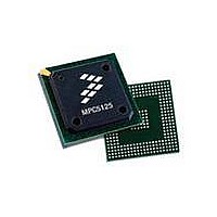
MPC5125YVN400 Freescale Semiconductor, MPC5125YVN400 Datasheet - Page 313

MPC5125YVN400
Manufacturer Part Number
MPC5125YVN400
Description
IC MCU 32BIT E300 324TEPBGA
Manufacturer
Freescale Semiconductor
Series
MPC51xxr
Datasheets
1.MPC5125YVN400.pdf
(92 pages)
2.MPC5125YVN400.pdf
(8 pages)
3.MPC5125YVN400.pdf
(2 pages)
4.MPC5125YVN400.pdf
(1064 pages)
Specifications of MPC5125YVN400
Core Processor
e300
Core Size
32-Bit
Speed
400MHz
Connectivity
CAN, EBI/EMI, Ethernet, I²C, USB OTG
Peripherals
DMA, WDT
Number Of I /o
64
Program Memory Type
ROMless
Ram Size
32K x 8
Voltage - Supply (vcc/vdd)
1.33 V ~ 1.47 V
Oscillator Type
External
Operating Temperature
-40°C ~ 125°C
Package / Case
324-PBGA
Processor Series
MPC51xx
Core
e300
Data Bus Width
32 bit
Development Tools By Supplier
TWR-MPC5125-KIT, TWR-SER, TWR-ELEV, TOWER
Maximum Clock Frequency
400 MHz
Operating Supply Voltage
1.4 V
Maximum Operating Temperature
+ 125 C
Mounting Style
SMD/SMT
Data Ram Size
32 KB
I/o Voltage
3.3 V
Interface Type
CAN, I2C
Minimum Operating Temperature
- 40 C
Program Memory Size
32 bit
Cpu Speed
400MHz
Embedded Interface Type
CAN, I2C, SPI, UART, USB
Digital Ic Case Style
TEPBGA
No. Of Pins
324
Rohs Compliant
Yes
Cpu Family
MPC5xx
Device Core Size
32b
Frequency (max)
400MHz
Total Internal Ram Size
32KB
Instruction Set Architecture
RISC
Operating Temp Range
-40C to 85C
Operating Temperature Classification
Industrial
Mounting
Surface Mount
Pin Count
324
Lead Free Status / RoHS Status
Lead free / RoHS Compliant
Eeprom Size
-
Program Memory Size
-
Data Converters
-
Lead Free Status / Rohs Status
Lead free / RoHS Compliant
Available stocks
Company
Part Number
Manufacturer
Quantity
Price
Company:
Part Number:
MPC5125YVN400
Manufacturer:
Freescale Semiconductor
Quantity:
135
Company:
Part Number:
MPC5125YVN400
Manufacturer:
LTC
Quantity:
29
Company:
Part Number:
MPC5125YVN400
Manufacturer:
Freescale Semiconductor
Quantity:
10 000
- MPC5125YVN400 PDF datasheet
- MPC5125YVN400 PDF datasheet #2
- MPC5125YVN400 PDF datasheet #3
- MPC5125YVN400 PDF datasheet #4
- Current page: 313 of 1064
- Download datasheet (6Mb)
11.3.2
11.3.2.1
Freescale Semiconductor
Address: Base + 0x0000
DRAM_BANK_SELECT
DRAM_ROW_SELECT
Reset
Reset
16-BIT MODE
READ_TEST
SELFREFEN
CMD MODE
W
W
R
R
CLK ON
RST_B
Field
RST_
CKE
and
16
B
0
0
0
Register Descriptions
RDLY[2:0]
DDR System Configuration Register (DDR_SYS_CONFIG)
CKE
17
0
0
1
Figure 11-2. DDR System Configuration Register (DDR_SYS_CONFIG)
CLK
ON
18
0
0
2
DRAM controller soft reset. When this bit is 0, the DRAM controller is in the reset state. When this
bit is 1, the DRAM controller is out of reset. The bit controls the reset to the internal state machines.
The configuration registers are reset by the resets from the hardware reset block, not by this bit.
Value on the DRAM CKE pin. For functional operation, this needs to be high. During power-down,
value can be low.
When this bit is 1, the DRAM clock is running. When this bit is 0, the DRAM clock is stopped
When this bit is 0, the DRAM controller is in normal operation. When this bit is 1, the DRAM controller
is in command mode and does not respond to requests on the incoming buses. Command mode is
used for DRAM initialization and to switch the DRAM into and out of the different power-down and
self-refresh modes.
These fields control the multiplexing of the bus address to the DRAM bank and row address.
Table 11-5
relationship is given in
These fields are for production test. Do not use.
Self-refresh enable. When this bit is 1, the DRAM controller autonomously enters and exits the
self-refresh using the self-refresh command registers when requested by the PMC. When the bit is
0, the transition is blocked.
When this bit is set, the DRAM controller assumes a 16-bit wide memory is used. When this bit is
cleared, a 32-bit wide memory is assumed.
Note: This does not configure the pins for 16-bit mode. That must be done in the pin configuration.
MODE
HALF
CMD
DQS
DLY
Table 11-2. DDR_SYS_CONFIG field descriptions
19
1
0
3
MPC5125 Microcontroller Reference Manual, Rev. 2
and
DRAM_ROW_SELECT
DQS
QUA
DLY
RT
20
4
0
0
Table 11-6
21
0
0
5
Table
WDLY[2:0]
give the details. DRAM column address depends on 16-bit mode bit, and
22
11-5.
0
0
6
DRAM_BANK_SELECT
23
0
0
7
EARL
ODT
Description
24
Y
8
0
0
NATE
TER
DIE
ON
MI-
25
9
0
0
CLEAR
FIFO
OV
10
26
0
0
CLEAR
READ_TEST
FIFO
UV
11
27
0
0
PEND
FIFO
OV
12
28
0
0
Access: User read/write
PEND FIFO
SELF
FIFO
REF
EN
UV
13
29
0
0
DRAM Controller
16BIT
MODE
OV
EN
14
30
0
0
RDLY
FIFO
UV
EN
[3]
15
31
11-5
0
0
Related parts for MPC5125YVN400
Image
Part Number
Description
Manufacturer
Datasheet
Request
R
Part Number:
Description:
Mpc5125 Microcontroller Data Sheet
Manufacturer:
Freescale Semiconductor, Inc
Datasheet:

Part Number:
Description:
MPC5125 Microcontroller Data Sheet
Manufacturer:
FREESCALE [Freescale Semiconductor, Inc]
Datasheet:
Part Number:
Description:
Manufacturer:
Freescale Semiconductor, Inc
Datasheet:
Part Number:
Description:
Manufacturer:
Freescale Semiconductor, Inc
Datasheet:
Part Number:
Description:
Manufacturer:
Freescale Semiconductor, Inc
Datasheet:
Part Number:
Description:
Manufacturer:
Freescale Semiconductor, Inc
Datasheet:
Part Number:
Description:
Manufacturer:
Freescale Semiconductor, Inc
Datasheet:
Part Number:
Description:
Manufacturer:
Freescale Semiconductor, Inc
Datasheet:
Part Number:
Description:
Manufacturer:
Freescale Semiconductor, Inc
Datasheet:
Part Number:
Description:
Manufacturer:
Freescale Semiconductor, Inc
Datasheet:
Part Number:
Description:
Manufacturer:
Freescale Semiconductor, Inc
Datasheet:
Part Number:
Description:
Manufacturer:
Freescale Semiconductor, Inc
Datasheet:
Part Number:
Description:
Manufacturer:
Freescale Semiconductor, Inc
Datasheet:
Part Number:
Description:
Manufacturer:
Freescale Semiconductor, Inc
Datasheet:
Part Number:
Description:
Manufacturer:
Freescale Semiconductor, Inc
Datasheet:


