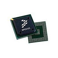
MPC5125YVN400 Freescale Semiconductor, MPC5125YVN400 Datasheet - Page 609

MPC5125YVN400
Manufacturer Part Number
MPC5125YVN400
Description
IC MCU 32BIT E300 324TEPBGA
Manufacturer
Freescale Semiconductor
Series
MPC51xxr
Datasheets
1.MPC5125YVN400.pdf
(92 pages)
2.MPC5125YVN400.pdf
(8 pages)
3.MPC5125YVN400.pdf
(2 pages)
4.MPC5125YVN400.pdf
(1064 pages)
Specifications of MPC5125YVN400
Core Processor
e300
Core Size
32-Bit
Speed
400MHz
Connectivity
CAN, EBI/EMI, Ethernet, I²C, USB OTG
Peripherals
DMA, WDT
Number Of I /o
64
Program Memory Type
ROMless
Ram Size
32K x 8
Voltage - Supply (vcc/vdd)
1.33 V ~ 1.47 V
Oscillator Type
External
Operating Temperature
-40°C ~ 125°C
Package / Case
324-PBGA
Processor Series
MPC51xx
Core
e300
Data Bus Width
32 bit
Development Tools By Supplier
TWR-MPC5125-KIT, TWR-SER, TWR-ELEV, TOWER
Maximum Clock Frequency
400 MHz
Operating Supply Voltage
1.4 V
Maximum Operating Temperature
+ 125 C
Mounting Style
SMD/SMT
Data Ram Size
32 KB
I/o Voltage
3.3 V
Interface Type
CAN, I2C
Minimum Operating Temperature
- 40 C
Program Memory Size
32 bit
Cpu Speed
400MHz
Embedded Interface Type
CAN, I2C, SPI, UART, USB
Digital Ic Case Style
TEPBGA
No. Of Pins
324
Rohs Compliant
Yes
Cpu Family
MPC5xx
Device Core Size
32b
Frequency (max)
400MHz
Total Internal Ram Size
32KB
Instruction Set Architecture
RISC
Operating Temp Range
-40C to 85C
Operating Temperature Classification
Industrial
Mounting
Surface Mount
Pin Count
324
Lead Free Status / RoHS Status
Lead free / RoHS Compliant
Eeprom Size
-
Program Memory Size
-
Data Converters
-
Lead Free Status / Rohs Status
Lead free / RoHS Compliant
Available stocks
Company
Part Number
Manufacturer
Quantity
Price
Company:
Part Number:
MPC5125YVN400
Manufacturer:
Freescale Semiconductor
Quantity:
135
Company:
Part Number:
MPC5125YVN400
Manufacturer:
LTC
Quantity:
29
Company:
Part Number:
MPC5125YVN400
Manufacturer:
Freescale Semiconductor
Quantity:
10 000
- MPC5125YVN400 PDF datasheet
- MPC5125YVN400 PDF datasheet #2
- MPC5125YVN400 PDF datasheet #3
- MPC5125YVN400 PDF datasheet #4
- Current page: 609 of 1064
- Download datasheet (6Mb)
1
22.3.3.2
The eight data segment registers, each with bits DB[7:0], contain the data to be transmitted or received.
The number of bytes to be transmitted or received is determined by the data length code in the
corresponding DLR register.
Freescale Semiconductor
Reset value is indeterminate.
Address: Base + 0x41 (RX)
Address: 0x48 (RX DSR0)
ID[2:0]
Field
RTR
Reset
Reset
IDE
W
W
R
R
1
1
Base + 0x61 (TX)
0x49 (RX DSR1)
0x4C (RX DSR2)
0x4D (RX DSR3)
0x50 (RX DSR4)
0x51 (RX DSR5)
0x54 (RX DSR6)
0x55 (RX DSR7)
Figure 22-28. Data Segment Registers (DSR0–DSR7)—Extended Identifier Mapping
Standard Format Identifier. The identifiers consist of 11 bits (ID[10:0]) for the standard format. ID10 is the most
significant bit and is transmitted first on the CAN bus during the arbitration procedure. The priority of an identifier
is defined to be highest for the smallest binary number. See also ID bits in
Remote Transmission Request. This flag reflects the status of the Remote Transmission Request bit in the CAN
frame. In the case of a receive buffer, it indicates the status of the received frame and supports the transmission
of an answering frame in software. In the case of a transmit buffer, this flag defines the setting of the RTR bit to
be sent.
0 Data frame.
1 Remote frame.
ID Extended. This flag indicates whether the extended or standard identifier format is applied in this buffer. In the
case of a receive buffer, the flag is set as received and indicates to the Power Architecture how to process the
buffer identifier registers. In the case of a transmit buffer, the flag indicates to the MSCAN what type of identifier
to send.
0 Standard format (11 bit).
1 Extended format (29 bit).
Data Segment Registers (DSR0–7)
DB7
ID2
—
—
0
0
Table 22-27. IDR1 Register Field Descriptions—Standard Mapping
Figure 22-27. Identifier Register 1 (IDR1)—Standard Mapping
DB6
ID1
—
—
1
1
MPC5125 Microcontroller Reference Manual, Rev. 2
0x68 (TX DSR0)
0x69 (TX DSR1)
0x6C (TX DSR2)
0x6D (TX DSR3)
0x70 (TX DSR4)
0x71 (TX DSR5)
0x74 (TX DSR6)
0x75 (TX DSR7)
DB5
ID0
—
—
2
2
RTR
DB4
—
—
3
3
Description
IDE (=0)
DB3
—
—
4
4
DB2
Table
—
—
5
5
22-26.
Access: User read/write
Access: User read/write
DB1
—
—
6
6
DB0
—
—
7
7
MSCAN
22-31
Related parts for MPC5125YVN400
Image
Part Number
Description
Manufacturer
Datasheet
Request
R
Part Number:
Description:
Mpc5125 Microcontroller Data Sheet
Manufacturer:
Freescale Semiconductor, Inc
Datasheet:

Part Number:
Description:
MPC5125 Microcontroller Data Sheet
Manufacturer:
FREESCALE [Freescale Semiconductor, Inc]
Datasheet:
Part Number:
Description:
Manufacturer:
Freescale Semiconductor, Inc
Datasheet:
Part Number:
Description:
Manufacturer:
Freescale Semiconductor, Inc
Datasheet:
Part Number:
Description:
Manufacturer:
Freescale Semiconductor, Inc
Datasheet:
Part Number:
Description:
Manufacturer:
Freescale Semiconductor, Inc
Datasheet:
Part Number:
Description:
Manufacturer:
Freescale Semiconductor, Inc
Datasheet:
Part Number:
Description:
Manufacturer:
Freescale Semiconductor, Inc
Datasheet:
Part Number:
Description:
Manufacturer:
Freescale Semiconductor, Inc
Datasheet:
Part Number:
Description:
Manufacturer:
Freescale Semiconductor, Inc
Datasheet:
Part Number:
Description:
Manufacturer:
Freescale Semiconductor, Inc
Datasheet:
Part Number:
Description:
Manufacturer:
Freescale Semiconductor, Inc
Datasheet:
Part Number:
Description:
Manufacturer:
Freescale Semiconductor, Inc
Datasheet:
Part Number:
Description:
Manufacturer:
Freescale Semiconductor, Inc
Datasheet:
Part Number:
Description:
Manufacturer:
Freescale Semiconductor, Inc
Datasheet:


