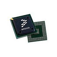
MPC5125YVN400 Freescale Semiconductor, MPC5125YVN400 Datasheet - Page 577

MPC5125YVN400
Manufacturer Part Number
MPC5125YVN400
Description
IC MCU 32BIT E300 324TEPBGA
Manufacturer
Freescale Semiconductor
Series
MPC51xxr
Datasheets
1.MPC5125YVN400.pdf
(92 pages)
2.MPC5125YVN400.pdf
(8 pages)
3.MPC5125YVN400.pdf
(2 pages)
4.MPC5125YVN400.pdf
(1064 pages)
Specifications of MPC5125YVN400
Core Processor
e300
Core Size
32-Bit
Speed
400MHz
Connectivity
CAN, EBI/EMI, Ethernet, I²C, USB OTG
Peripherals
DMA, WDT
Number Of I /o
64
Program Memory Type
ROMless
Ram Size
32K x 8
Voltage - Supply (vcc/vdd)
1.33 V ~ 1.47 V
Oscillator Type
External
Operating Temperature
-40°C ~ 125°C
Package / Case
324-PBGA
Processor Series
MPC51xx
Core
e300
Data Bus Width
32 bit
Development Tools By Supplier
TWR-MPC5125-KIT, TWR-SER, TWR-ELEV, TOWER
Maximum Clock Frequency
400 MHz
Operating Supply Voltage
1.4 V
Maximum Operating Temperature
+ 125 C
Mounting Style
SMD/SMT
Data Ram Size
32 KB
I/o Voltage
3.3 V
Interface Type
CAN, I2C
Minimum Operating Temperature
- 40 C
Program Memory Size
32 bit
Cpu Speed
400MHz
Embedded Interface Type
CAN, I2C, SPI, UART, USB
Digital Ic Case Style
TEPBGA
No. Of Pins
324
Rohs Compliant
Yes
Cpu Family
MPC5xx
Device Core Size
32b
Frequency (max)
400MHz
Total Internal Ram Size
32KB
Instruction Set Architecture
RISC
Operating Temp Range
-40C to 85C
Operating Temperature Classification
Industrial
Mounting
Surface Mount
Pin Count
324
Lead Free Status / RoHS Status
Lead free / RoHS Compliant
Eeprom Size
-
Program Memory Size
-
Data Converters
-
Lead Free Status / Rohs Status
Lead free / RoHS Compliant
Available stocks
Company
Part Number
Manufacturer
Quantity
Price
Company:
Part Number:
MPC5125YVN400
Manufacturer:
Freescale Semiconductor
Quantity:
135
Company:
Part Number:
MPC5125YVN400
Manufacturer:
LTC
Quantity:
29
Company:
Part Number:
MPC5125YVN400
Manufacturer:
Freescale Semiconductor
Quantity:
10 000
- MPC5125YVN400 PDF datasheet
- MPC5125YVN400 PDF datasheet #2
- MPC5125YVN400 PDF datasheet #3
- MPC5125YVN400 PDF datasheet #4
- Current page: 577 of 1064
- Download datasheet (6Mb)
To execute code from CS0 instead of CSBoot, the CS0 access window register must be configured and a
jump instruction into this address space needs to be executed.
Deadcycles from 0 to 3 can be added to any CS read access and occur in addition to any cycles that already
exist. The chip select deadcycle control register configures deadcycles.
Holdcycles from 0 to 3 can be added to any CS write access and occur in addition to any cycles that already
exist.
Burst mode operations are supported on all CSs and all modes and can be configured by the chip select
burst control register.
The following features are valid for all CSs and for both modes (non-muxed and muxed):
Asynchronous burst mode (Page mode) is supported in non-muxed mode.
21.3.3
The SCLPC interface, together with the DMA engine, can be used to transfer data between an external
device and the DRAM without the usage of the e300 processor.
SCLPC controls the data transfer between the LPC RX/TX FIFO and the external device. The external
transfer behavior is defined by the CSBoot/CS[x] configuration, chip select burst control, chip select
deadcycle, and chip select holdcycle registers. The supported transfer sizes are limited, by BPT bit field
setting, to 1, 2, 4, 8, 16, 24, 32, 40, 48, or 56 bytes only. Burst transfers could be generated with transfer
size settings greater as 4.
The SCLPC controller supports half-duplex operation (transmit or receive) only. If software configures a
transmit packet, the packet must be complete before a receive operation can be configured and started. The
length of one transfer packet is defined with the Packet Size bit field of the SCLPC Packet Size
(LPC_SCLPC_PS) Register. A transfer packet is split down into smaller bytes-per-transfer (BPT) slice. A
BPT slice cannot be interrupted by a direct e300 access to an external device. A BPT slice needs to be
finished first before the e300 access goes onto the external bus.
21.3.3.1
The device-specific behavior (non-/muxed, burst, wait
be programmed before the SCLPC is set up.
Freescale Semiconductor
•
•
•
•
•
Supports 8-, 16-, and 32-bit data bus width
Supports dynamic bus sizing, which means read and write transactions greater than the defined port
size are possible
Transactions less than the defined port size are supported only if the device can decode the
Tsiz[1:0] bits, which indicate the current transaction size.
Supports code execution
— The e300 processor can execute code from the LP bus from all CS
Supports burst access (read and write)
— Synchronous burst
SCLPC Interface
SCLPC Programming
MPC5125 Microcontroller Reference Manual, Rev. 2
cycles—Table 21-3
through
LocalPlus Bus Controller (LPC)
Table
21-11) needs to
21-37
Related parts for MPC5125YVN400
Image
Part Number
Description
Manufacturer
Datasheet
Request
R
Part Number:
Description:
Mpc5125 Microcontroller Data Sheet
Manufacturer:
Freescale Semiconductor, Inc
Datasheet:

Part Number:
Description:
MPC5125 Microcontroller Data Sheet
Manufacturer:
FREESCALE [Freescale Semiconductor, Inc]
Datasheet:
Part Number:
Description:
Manufacturer:
Freescale Semiconductor, Inc
Datasheet:
Part Number:
Description:
Manufacturer:
Freescale Semiconductor, Inc
Datasheet:
Part Number:
Description:
Manufacturer:
Freescale Semiconductor, Inc
Datasheet:
Part Number:
Description:
Manufacturer:
Freescale Semiconductor, Inc
Datasheet:
Part Number:
Description:
Manufacturer:
Freescale Semiconductor, Inc
Datasheet:
Part Number:
Description:
Manufacturer:
Freescale Semiconductor, Inc
Datasheet:
Part Number:
Description:
Manufacturer:
Freescale Semiconductor, Inc
Datasheet:
Part Number:
Description:
Manufacturer:
Freescale Semiconductor, Inc
Datasheet:
Part Number:
Description:
Manufacturer:
Freescale Semiconductor, Inc
Datasheet:
Part Number:
Description:
Manufacturer:
Freescale Semiconductor, Inc
Datasheet:
Part Number:
Description:
Manufacturer:
Freescale Semiconductor, Inc
Datasheet:
Part Number:
Description:
Manufacturer:
Freescale Semiconductor, Inc
Datasheet:
Part Number:
Description:
Manufacturer:
Freescale Semiconductor, Inc
Datasheet:


