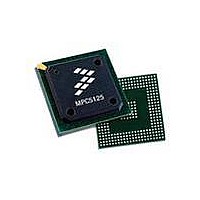
MPC5125YVN400 Freescale Semiconductor, MPC5125YVN400 Datasheet - Page 305

MPC5125YVN400
Manufacturer Part Number
MPC5125YVN400
Description
IC MCU 32BIT E300 324TEPBGA
Manufacturer
Freescale Semiconductor
Series
MPC51xxr
Datasheets
1.MPC5125YVN400.pdf
(92 pages)
2.MPC5125YVN400.pdf
(8 pages)
3.MPC5125YVN400.pdf
(2 pages)
4.MPC5125YVN400.pdf
(1064 pages)
Specifications of MPC5125YVN400
Core Processor
e300
Core Size
32-Bit
Speed
400MHz
Connectivity
CAN, EBI/EMI, Ethernet, I²C, USB OTG
Peripherals
DMA, WDT
Number Of I /o
64
Program Memory Type
ROMless
Ram Size
32K x 8
Voltage - Supply (vcc/vdd)
1.33 V ~ 1.47 V
Oscillator Type
External
Operating Temperature
-40°C ~ 125°C
Package / Case
324-PBGA
Processor Series
MPC51xx
Core
e300
Data Bus Width
32 bit
Development Tools By Supplier
TWR-MPC5125-KIT, TWR-SER, TWR-ELEV, TOWER
Maximum Clock Frequency
400 MHz
Operating Supply Voltage
1.4 V
Maximum Operating Temperature
+ 125 C
Mounting Style
SMD/SMT
Data Ram Size
32 KB
I/o Voltage
3.3 V
Interface Type
CAN, I2C
Minimum Operating Temperature
- 40 C
Program Memory Size
32 bit
Cpu Speed
400MHz
Embedded Interface Type
CAN, I2C, SPI, UART, USB
Digital Ic Case Style
TEPBGA
No. Of Pins
324
Rohs Compliant
Yes
Cpu Family
MPC5xx
Device Core Size
32b
Frequency (max)
400MHz
Total Internal Ram Size
32KB
Instruction Set Architecture
RISC
Operating Temp Range
-40C to 85C
Operating Temperature Classification
Industrial
Mounting
Surface Mount
Pin Count
324
Lead Free Status / RoHS Status
Lead free / RoHS Compliant
Eeprom Size
-
Program Memory Size
-
Data Converters
-
Lead Free Status / Rohs Status
Lead free / RoHS Compliant
Available stocks
Company
Part Number
Manufacturer
Quantity
Price
Company:
Part Number:
MPC5125YVN400
Manufacturer:
Freescale Semiconductor
Quantity:
135
Company:
Part Number:
MPC5125YVN400
Manufacturer:
LTC
Quantity:
29
Company:
Part Number:
MPC5125YVN400
Manufacturer:
Freescale Semiconductor
Quantity:
10 000
- MPC5125YVN400 PDF datasheet
- MPC5125YVN400 PDF datasheet #2
- MPC5125YVN400 PDF datasheet #3
- MPC5125YVN400 PDF datasheet #4
- Current page: 305 of 1064
- Download datasheet (6Mb)
Display Interface Unit (DIU)
(PRIORITY_0 to PRIORITY_7 from high to low). The priority value ranges from 0 to 15 and accesses
are blocked if the priority value is 0.
To use option 2, it is recommended to program PRIOMAN_CONFIG2[LUT SEL0] to 3, so that the
priority manager selects the alternate look-up table for the DIU if DIU incoming priority bit 3 is high. So
the user can set the DIU priority low in the main look-up table and set it high in the alternate look-up table,
and program the PLUT register so for example its priority bit 3 is high (0x8) when the buffer is lower than
half full. The purpose to do this is to only escalate the DIU priority when necessary, and save the DRAM
bandwidth to the other masters like the Power Architecture e300 core.
10.4.13 Display Signal Timing
The first step to generate appropriate timing signals for the selected display is to adjust the frequency of
the pixel clock to a frequency within the specified parameters of the display (see
Section 10.4.13.1,
“Refresh
Rate”). Program the SCFR1 register in the system clock module, SCFR1[DIU_DIV], to set the
divide ratio for the DIU pixel clock (refer to the system clock chapter).
Then the horizontal and vertical synchronize signals are generated based on the pixel clock. The
relationship between pixel clock, HSYNC, and VSYNC signals is shown in diagram
Figure 10-49
and
Figure
10-50.
Refer to
Section 10.3.3.11, “Display Size Register (DISP_SIZE),” Section 10.3.3.14, “Horizontal Sync
Pulse Parameters Register (HSYN_PARA),” Section 10.3.3.15, “Vertical Sync Pulse Parameters Register
(VSYN_PARA),”
and
Section 10.3.3.16, “Synchronization Signals Polarity Register (SYN_POL),”
for
related display parameter configuration registers.
Figure 10-49. Horizontal Sync Signals
MPC5125 Microcontroller Reference Manual, Rev. 2
Freescale Semiconductor
10-43
Related parts for MPC5125YVN400
Image
Part Number
Description
Manufacturer
Datasheet
Request
R
Part Number:
Description:
Mpc5125 Microcontroller Data Sheet
Manufacturer:
Freescale Semiconductor, Inc
Datasheet:

Part Number:
Description:
MPC5125 Microcontroller Data Sheet
Manufacturer:
FREESCALE [Freescale Semiconductor, Inc]
Datasheet:
Part Number:
Description:
Manufacturer:
Freescale Semiconductor, Inc
Datasheet:
Part Number:
Description:
Manufacturer:
Freescale Semiconductor, Inc
Datasheet:
Part Number:
Description:
Manufacturer:
Freescale Semiconductor, Inc
Datasheet:
Part Number:
Description:
Manufacturer:
Freescale Semiconductor, Inc
Datasheet:
Part Number:
Description:
Manufacturer:
Freescale Semiconductor, Inc
Datasheet:
Part Number:
Description:
Manufacturer:
Freescale Semiconductor, Inc
Datasheet:
Part Number:
Description:
Manufacturer:
Freescale Semiconductor, Inc
Datasheet:
Part Number:
Description:
Manufacturer:
Freescale Semiconductor, Inc
Datasheet:
Part Number:
Description:
Manufacturer:
Freescale Semiconductor, Inc
Datasheet:
Part Number:
Description:
Manufacturer:
Freescale Semiconductor, Inc
Datasheet:
Part Number:
Description:
Manufacturer:
Freescale Semiconductor, Inc
Datasheet:
Part Number:
Description:
Manufacturer:
Freescale Semiconductor, Inc
Datasheet:
Part Number:
Description:
Manufacturer:
Freescale Semiconductor, Inc
Datasheet:


