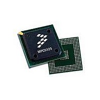
MPC5125YVN400 Freescale Semiconductor, MPC5125YVN400 Datasheet - Page 873

MPC5125YVN400
Manufacturer Part Number
MPC5125YVN400
Description
IC MCU 32BIT E300 324TEPBGA
Manufacturer
Freescale Semiconductor
Series
MPC51xxr
Datasheets
1.MPC5125YVN400.pdf
(92 pages)
2.MPC5125YVN400.pdf
(8 pages)
3.MPC5125YVN400.pdf
(2 pages)
4.MPC5125YVN400.pdf
(1064 pages)
Specifications of MPC5125YVN400
Core Processor
e300
Core Size
32-Bit
Speed
400MHz
Connectivity
CAN, EBI/EMI, Ethernet, I²C, USB OTG
Peripherals
DMA, WDT
Number Of I /o
64
Program Memory Type
ROMless
Ram Size
32K x 8
Voltage - Supply (vcc/vdd)
1.33 V ~ 1.47 V
Oscillator Type
External
Operating Temperature
-40°C ~ 125°C
Package / Case
324-PBGA
Processor Series
MPC51xx
Core
e300
Data Bus Width
32 bit
Development Tools By Supplier
TWR-MPC5125-KIT, TWR-SER, TWR-ELEV, TOWER
Maximum Clock Frequency
400 MHz
Operating Supply Voltage
1.4 V
Maximum Operating Temperature
+ 125 C
Mounting Style
SMD/SMT
Data Ram Size
32 KB
I/o Voltage
3.3 V
Interface Type
CAN, I2C
Minimum Operating Temperature
- 40 C
Program Memory Size
32 bit
Cpu Speed
400MHz
Embedded Interface Type
CAN, I2C, SPI, UART, USB
Digital Ic Case Style
TEPBGA
No. Of Pins
324
Rohs Compliant
Yes
Cpu Family
MPC5xx
Device Core Size
32b
Frequency (max)
400MHz
Total Internal Ram Size
32KB
Instruction Set Architecture
RISC
Operating Temp Range
-40C to 85C
Operating Temperature Classification
Industrial
Mounting
Surface Mount
Pin Count
324
Lead Free Status / RoHS Status
Lead free / RoHS Compliant
Eeprom Size
-
Program Memory Size
-
Data Converters
-
Lead Free Status / Rohs Status
Lead free / RoHS Compliant
Available stocks
Company
Part Number
Manufacturer
Quantity
Price
Company:
Part Number:
MPC5125YVN400
Manufacturer:
Freescale Semiconductor
Quantity:
135
Company:
Part Number:
MPC5125YVN400
Manufacturer:
LTC
Quantity:
29
Company:
Part Number:
MPC5125YVN400
Manufacturer:
Freescale Semiconductor
Quantity:
10 000
- MPC5125YVN400 PDF datasheet
- MPC5125YVN400 PDF datasheet #2
- MPC5125YVN400 PDF datasheet #3
- MPC5125YVN400 PDF datasheet #4
- Current page: 873 of 1064
- Download datasheet (6Mb)
Freescale Semiconductor
Address: Base + 0x1A8
Reset
Reset
SLOM
VBPS
Field
SDIS
ES
W
W
R
R
16
0
0
0
0
0
Vbus Power Select (0—Output is 0; 1—Output is one)
This bit is connected to the vbus_pwr_select output and can be used for any generic control but is named to
be used by logic that selects between an on-chip Vbus power source (charge pump) and an off-chip source
in systems when both are available.
Stream Disable.
In host mode, setting this bit to a 1 ensures that overruns/underruns of the latency FIFO are eliminated for low
bandwidth systems where the RX and TX buffers are sufficient to contain the entire packet. Enabling stream
disable also has the effect of ensuring the TX latency is filled to capacity before the packet is launched onto
the USB.
Time duration to pre-fill the FIFO becomes significant when stream disable is active. See
USB_TXFILLTUNING to characterize the adjustments needed for the scheduler when using this feature.
In systems with high system bus utilization, setting this bit ensures no overruns or underruns during operation
at the expense of link utilization. For those who desire optimal link performance, SDIS can be left clear, and
the rules used under the description of the USB_TXFILLTUNING register to limit underruns/overruns.
0 Inactive.
1 Active.
In device mode, setting this bit to a 1 disables double priming on both RX and TX for low bandwidth systems.
This mode ensures that when the RX and TX buffers are sufficient to contain an entire packet, the standard
double buffering scheme is disabled to prevent overruns/underruns in bandwidth limited systems.
In high speed mode, all packets received are responded to with a NYET handshake when stream disable is
active.
Setup Lockout Mode. For the OTG module in device mode, this bit controls behavior of the setup lock
mechanism. See
0 Setup Lockouts On.
1 Setup Lockouts Off (DCD requires use of Setup Data Buffer Tripwire in USB_USBCMD).
Endian Select.
This bit can change the byte ordering of the transfer buffers to match the host microprocessor bus architecture.
The bit fields in the microprocessor interface and the DMA data structures (including the setup buffer within
the device QH) are unaffected by the value of this bit, because they are based upon 32-bit words.
0 Little Endian—[Default]: first byte referenced in least significant byte of 32-bit word.
1 Big Endian—first byte referenced in most significant byte of 32-bit word.
17
0
0
0
0
1
18
0
0
0
0
2
Figure 32-33. USB Mode (USB_USBMODE) Register
19
0
0
0
0
3
Table 32-34. USB_USBMODE field descriptions
Section 32.8.5.2, “Control Endpoint Operation Model.”
MPC5125 Microcontroller Reference Manual, Rev. 2
20
4
0
0
0
0
21
0
0
0
0
5
22
0
0
0
0
6
23
0
0
0
0
7
Description
24
8
0
0
0
0
25
9
0
0
0
0
Universal Serial Bus Interface with On-The-Go
VBPS SDIS SLOM
10
26
0
0
0
11
27
0
0
0
12
28
0
0
0
Access: User read/write
ES
13
29
0
0
0
14
30
0
0
0
CM
32-45
15
31
0
0
0
Related parts for MPC5125YVN400
Image
Part Number
Description
Manufacturer
Datasheet
Request
R
Part Number:
Description:
Mpc5125 Microcontroller Data Sheet
Manufacturer:
Freescale Semiconductor, Inc
Datasheet:

Part Number:
Description:
MPC5125 Microcontroller Data Sheet
Manufacturer:
FREESCALE [Freescale Semiconductor, Inc]
Datasheet:
Part Number:
Description:
Manufacturer:
Freescale Semiconductor, Inc
Datasheet:
Part Number:
Description:
Manufacturer:
Freescale Semiconductor, Inc
Datasheet:
Part Number:
Description:
Manufacturer:
Freescale Semiconductor, Inc
Datasheet:
Part Number:
Description:
Manufacturer:
Freescale Semiconductor, Inc
Datasheet:
Part Number:
Description:
Manufacturer:
Freescale Semiconductor, Inc
Datasheet:
Part Number:
Description:
Manufacturer:
Freescale Semiconductor, Inc
Datasheet:
Part Number:
Description:
Manufacturer:
Freescale Semiconductor, Inc
Datasheet:
Part Number:
Description:
Manufacturer:
Freescale Semiconductor, Inc
Datasheet:
Part Number:
Description:
Manufacturer:
Freescale Semiconductor, Inc
Datasheet:
Part Number:
Description:
Manufacturer:
Freescale Semiconductor, Inc
Datasheet:
Part Number:
Description:
Manufacturer:
Freescale Semiconductor, Inc
Datasheet:
Part Number:
Description:
Manufacturer:
Freescale Semiconductor, Inc
Datasheet:
Part Number:
Description:
Manufacturer:
Freescale Semiconductor, Inc
Datasheet:


