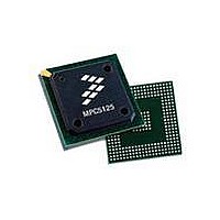
MPC5125YVN400 Freescale Semiconductor, MPC5125YVN400 Datasheet - Page 496

MPC5125YVN400
Manufacturer Part Number
MPC5125YVN400
Description
IC MCU 32BIT E300 324TEPBGA
Manufacturer
Freescale Semiconductor
Series
MPC51xxr
Datasheets
1.MPC5125YVN400.pdf
(92 pages)
2.MPC5125YVN400.pdf
(8 pages)
3.MPC5125YVN400.pdf
(2 pages)
4.MPC5125YVN400.pdf
(1064 pages)
Specifications of MPC5125YVN400
Core Processor
e300
Core Size
32-Bit
Speed
400MHz
Connectivity
CAN, EBI/EMI, Ethernet, I²C, USB OTG
Peripherals
DMA, WDT
Number Of I /o
64
Program Memory Type
ROMless
Ram Size
32K x 8
Voltage - Supply (vcc/vdd)
1.33 V ~ 1.47 V
Oscillator Type
External
Operating Temperature
-40°C ~ 125°C
Package / Case
324-PBGA
Processor Series
MPC51xx
Core
e300
Data Bus Width
32 bit
Development Tools By Supplier
TWR-MPC5125-KIT, TWR-SER, TWR-ELEV, TOWER
Maximum Clock Frequency
400 MHz
Operating Supply Voltage
1.4 V
Maximum Operating Temperature
+ 125 C
Mounting Style
SMD/SMT
Data Ram Size
32 KB
I/o Voltage
3.3 V
Interface Type
CAN, I2C
Minimum Operating Temperature
- 40 C
Program Memory Size
32 bit
Cpu Speed
400MHz
Embedded Interface Type
CAN, I2C, SPI, UART, USB
Digital Ic Case Style
TEPBGA
No. Of Pins
324
Rohs Compliant
Yes
Cpu Family
MPC5xx
Device Core Size
32b
Frequency (max)
400MHz
Total Internal Ram Size
32KB
Instruction Set Architecture
RISC
Operating Temp Range
-40C to 85C
Operating Temperature Classification
Industrial
Mounting
Surface Mount
Pin Count
324
Lead Free Status / RoHS Status
Lead free / RoHS Compliant
Eeprom Size
-
Program Memory Size
-
Data Converters
-
Lead Free Status / Rohs Status
Lead free / RoHS Compliant
Available stocks
Company
Part Number
Manufacturer
Quantity
Price
Company:
Part Number:
MPC5125YVN400
Manufacturer:
Freescale Semiconductor
Quantity:
135
Company:
Part Number:
MPC5125YVN400
Manufacturer:
LTC
Quantity:
29
Company:
Part Number:
MPC5125YVN400
Manufacturer:
Freescale Semiconductor
Quantity:
10 000
- MPC5125YVN400 PDF datasheet
- MPC5125YVN400 PDF datasheet #2
- MPC5125YVN400 PDF datasheet #3
- MPC5125YVN400 PDF datasheet #4
- Current page: 496 of 1064
- Download datasheet (6Mb)
Inter-Integrated Circuit (I
19.1.4
A STOP signal is a low-to-high transition of SDA while SCL is high.
The master generates a STOP signal to terminate communication, which frees the bus. The master can
generate a STOP even if the slave has generated an acknowledge, at which point the slave must release the
bus.
The master can generate a repeated start and address for other devices. At this time, the bus remains busy
if a repeated start is generated instead of a stop.
19.1.4.1
The first byte of data transferred by the master immediately after a START signal is the slave address. This
is a 7-bit calling address followed by a R/
transfer.
Only a slave with a calling address matching the address transmitted by the master responds by sending
back an acknowledge bit. This is done by pulling SDA low at the ninth clock as shown in
19.1.4.2
Data transfer proceeds byte-by-byte in a direction specified by the R/
data byte is 8 bits long. Data may be changed only while SCL is low and must be held stable while SCL
is high.
There is one clock pulse on SCL for each data bit. The MSB is transferred first. Each data byte must be
followed by an acknowledge bit signalled from the receiving device by pulling SDA low at the ninth clock.
One complete 8-bit data byte transfer needs nine clock pulses as shown in
19-4
•
•
SCL
SDA
Start
0 = Master writes data (W), becomes transmitter
1 = Master reads data (R), becomes receiver
STOP Signal
Slave Address Transmission
Data Transfer
Figure 19-2. Timing Diagram–Start, Address Transfer and Stop Signal
Bit7
2
1
C)
Bit6
2
MPC5125 Microcontroller Reference Manual, Rev. 2
MASTER Drives Data and Clock Lines
Bit5
3
W
Bit4
4
bit. The R/
Bit3
5
W
bit tells the slave the desired direction of data
Bit2
6
Bit1
W
7
bit sent by the calling master. Each
Bit0(R/W)
Slave Drives SDA Low
Figure
Master Release SDA
8
Ack Bit
19-3.
Release SDA
Freescale Semiconductor
9
Slave
Figure
19-2.
Stop
Related parts for MPC5125YVN400
Image
Part Number
Description
Manufacturer
Datasheet
Request
R
Part Number:
Description:
Mpc5125 Microcontroller Data Sheet
Manufacturer:
Freescale Semiconductor, Inc
Datasheet:

Part Number:
Description:
MPC5125 Microcontroller Data Sheet
Manufacturer:
FREESCALE [Freescale Semiconductor, Inc]
Datasheet:
Part Number:
Description:
Manufacturer:
Freescale Semiconductor, Inc
Datasheet:
Part Number:
Description:
Manufacturer:
Freescale Semiconductor, Inc
Datasheet:
Part Number:
Description:
Manufacturer:
Freescale Semiconductor, Inc
Datasheet:
Part Number:
Description:
Manufacturer:
Freescale Semiconductor, Inc
Datasheet:
Part Number:
Description:
Manufacturer:
Freescale Semiconductor, Inc
Datasheet:
Part Number:
Description:
Manufacturer:
Freescale Semiconductor, Inc
Datasheet:
Part Number:
Description:
Manufacturer:
Freescale Semiconductor, Inc
Datasheet:
Part Number:
Description:
Manufacturer:
Freescale Semiconductor, Inc
Datasheet:
Part Number:
Description:
Manufacturer:
Freescale Semiconductor, Inc
Datasheet:
Part Number:
Description:
Manufacturer:
Freescale Semiconductor, Inc
Datasheet:
Part Number:
Description:
Manufacturer:
Freescale Semiconductor, Inc
Datasheet:
Part Number:
Description:
Manufacturer:
Freescale Semiconductor, Inc
Datasheet:
Part Number:
Description:
Manufacturer:
Freescale Semiconductor, Inc
Datasheet:


