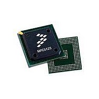
MPC5125YVN400 Freescale Semiconductor, MPC5125YVN400 Datasheet - Page 309

MPC5125YVN400
Manufacturer Part Number
MPC5125YVN400
Description
IC MCU 32BIT E300 324TEPBGA
Manufacturer
Freescale Semiconductor
Series
MPC51xxr
Datasheets
1.MPC5125YVN400.pdf
(92 pages)
2.MPC5125YVN400.pdf
(8 pages)
3.MPC5125YVN400.pdf
(2 pages)
4.MPC5125YVN400.pdf
(1064 pages)
Specifications of MPC5125YVN400
Core Processor
e300
Core Size
32-Bit
Speed
400MHz
Connectivity
CAN, EBI/EMI, Ethernet, I²C, USB OTG
Peripherals
DMA, WDT
Number Of I /o
64
Program Memory Type
ROMless
Ram Size
32K x 8
Voltage - Supply (vcc/vdd)
1.33 V ~ 1.47 V
Oscillator Type
External
Operating Temperature
-40°C ~ 125°C
Package / Case
324-PBGA
Processor Series
MPC51xx
Core
e300
Data Bus Width
32 bit
Development Tools By Supplier
TWR-MPC5125-KIT, TWR-SER, TWR-ELEV, TOWER
Maximum Clock Frequency
400 MHz
Operating Supply Voltage
1.4 V
Maximum Operating Temperature
+ 125 C
Mounting Style
SMD/SMT
Data Ram Size
32 KB
I/o Voltage
3.3 V
Interface Type
CAN, I2C
Minimum Operating Temperature
- 40 C
Program Memory Size
32 bit
Cpu Speed
400MHz
Embedded Interface Type
CAN, I2C, SPI, UART, USB
Digital Ic Case Style
TEPBGA
No. Of Pins
324
Rohs Compliant
Yes
Cpu Family
MPC5xx
Device Core Size
32b
Frequency (max)
400MHz
Total Internal Ram Size
32KB
Instruction Set Architecture
RISC
Operating Temp Range
-40C to 85C
Operating Temperature Classification
Industrial
Mounting
Surface Mount
Pin Count
324
Lead Free Status / RoHS Status
Lead free / RoHS Compliant
Eeprom Size
-
Program Memory Size
-
Data Converters
-
Lead Free Status / Rohs Status
Lead free / RoHS Compliant
Available stocks
Company
Part Number
Manufacturer
Quantity
Price
Company:
Part Number:
MPC5125YVN400
Manufacturer:
Freescale Semiconductor
Quantity:
135
Company:
Part Number:
MPC5125YVN400
Manufacturer:
LTC
Quantity:
29
Company:
Part Number:
MPC5125YVN400
Manufacturer:
Freescale Semiconductor
Quantity:
10 000
- MPC5125YVN400 PDF datasheet
- MPC5125YVN400 PDF datasheet #2
- MPC5125YVN400 PDF datasheet #3
- MPC5125YVN400 PDF datasheet #4
- Current page: 309 of 1064
- Download datasheet (6Mb)
Chapter 11
DRAM Controller
11.1
The DDR DRAM controller is a multi-port DRAM controller (four ports). It supports Mobile-DDR
DDR-1, DDR-2, and SDR memories.
A block diagram of the multi-port DRAM controller is given in
11.1.1
The DRAM controller is a multi-port controller that listens to incoming requests on the four incoming
buses and decides on each rising clock edge what command needs to be sent to the DRAM.
Each incoming bus is a 64-bit bus. The four incoming buses are:
The block supports connection of two DRAM rank (two chip selects) and supports the four major classes
of DRAM:
It supports these memories in 16-bit or 32-bit wide configurations. SDR is supported in only 32-bit wide
configuration.
The DRAM controller listens to the incoming requests to the four buses in parallel and then sends
commands to the DRAM from the highest priority bus at the current time, while the DRAM is ready to
receive the command from this particular bus. If the DRAM is blocked because it needs to meet a timing
requirement, the controller sends a command from a bus where there is no blockage.
For example, suppose bus one has an incoming request on priority four, and it hits in bank 1 and the page
is not open (the bank needs a precharge+activate command before the request can be serviced). Bus two
has an incoming request on priority five, it hits in bank two and the correct page is already open. In this
case, the DRAM controller accepts the bus two request first. While it is reading from the appropriate bank,
1. JEDEC standard calls these LPDDR. Most DRAM vendors call them Mobile-DDR.
Freescale Semiconductor
•
•
•
•
•
•
•
•
Bus 0: the DIU
Bus 1: the Power Architecture e300 core
Bus 2: NFC nand flash controller
Bus 3: DMA, USB, FEC
Mobile-DDR (LPDDR)
DDR1
DDR2
SDR
Introduction
Overview
MPC5125 Microcontroller Reference Manual, Rev. 2
Figure
11-1.
1
,
11-1
Related parts for MPC5125YVN400
Image
Part Number
Description
Manufacturer
Datasheet
Request
R
Part Number:
Description:
Mpc5125 Microcontroller Data Sheet
Manufacturer:
Freescale Semiconductor, Inc
Datasheet:

Part Number:
Description:
MPC5125 Microcontroller Data Sheet
Manufacturer:
FREESCALE [Freescale Semiconductor, Inc]
Datasheet:
Part Number:
Description:
Manufacturer:
Freescale Semiconductor, Inc
Datasheet:
Part Number:
Description:
Manufacturer:
Freescale Semiconductor, Inc
Datasheet:
Part Number:
Description:
Manufacturer:
Freescale Semiconductor, Inc
Datasheet:
Part Number:
Description:
Manufacturer:
Freescale Semiconductor, Inc
Datasheet:
Part Number:
Description:
Manufacturer:
Freescale Semiconductor, Inc
Datasheet:
Part Number:
Description:
Manufacturer:
Freescale Semiconductor, Inc
Datasheet:
Part Number:
Description:
Manufacturer:
Freescale Semiconductor, Inc
Datasheet:
Part Number:
Description:
Manufacturer:
Freescale Semiconductor, Inc
Datasheet:
Part Number:
Description:
Manufacturer:
Freescale Semiconductor, Inc
Datasheet:
Part Number:
Description:
Manufacturer:
Freescale Semiconductor, Inc
Datasheet:
Part Number:
Description:
Manufacturer:
Freescale Semiconductor, Inc
Datasheet:
Part Number:
Description:
Manufacturer:
Freescale Semiconductor, Inc
Datasheet:
Part Number:
Description:
Manufacturer:
Freescale Semiconductor, Inc
Datasheet:


