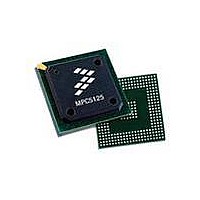
MPC5125YVN400 Freescale Semiconductor, MPC5125YVN400 Datasheet - Page 652

MPC5125YVN400
Manufacturer Part Number
MPC5125YVN400
Description
IC MCU 32BIT E300 324TEPBGA
Manufacturer
Freescale Semiconductor
Series
MPC51xxr
Datasheets
1.MPC5125YVN400.pdf
(92 pages)
2.MPC5125YVN400.pdf
(8 pages)
3.MPC5125YVN400.pdf
(2 pages)
4.MPC5125YVN400.pdf
(1064 pages)
Specifications of MPC5125YVN400
Core Processor
e300
Core Size
32-Bit
Speed
400MHz
Connectivity
CAN, EBI/EMI, Ethernet, I²C, USB OTG
Peripherals
DMA, WDT
Number Of I /o
64
Program Memory Type
ROMless
Ram Size
32K x 8
Voltage - Supply (vcc/vdd)
1.33 V ~ 1.47 V
Oscillator Type
External
Operating Temperature
-40°C ~ 125°C
Package / Case
324-PBGA
Processor Series
MPC51xx
Core
e300
Data Bus Width
32 bit
Development Tools By Supplier
TWR-MPC5125-KIT, TWR-SER, TWR-ELEV, TOWER
Maximum Clock Frequency
400 MHz
Operating Supply Voltage
1.4 V
Maximum Operating Temperature
+ 125 C
Mounting Style
SMD/SMT
Data Ram Size
32 KB
I/o Voltage
3.3 V
Interface Type
CAN, I2C
Minimum Operating Temperature
- 40 C
Program Memory Size
32 bit
Cpu Speed
400MHz
Embedded Interface Type
CAN, I2C, SPI, UART, USB
Digital Ic Case Style
TEPBGA
No. Of Pins
324
Rohs Compliant
Yes
Cpu Family
MPC5xx
Device Core Size
32b
Frequency (max)
400MHz
Total Internal Ram Size
32KB
Instruction Set Architecture
RISC
Operating Temp Range
-40C to 85C
Operating Temperature Classification
Industrial
Mounting
Surface Mount
Pin Count
324
Lead Free Status / RoHS Status
Lead free / RoHS Compliant
Eeprom Size
-
Program Memory Size
-
Data Converters
-
Lead Free Status / Rohs Status
Lead free / RoHS Compliant
Available stocks
Company
Part Number
Manufacturer
Quantity
Price
Company:
Part Number:
MPC5125YVN400
Manufacturer:
Freescale Semiconductor
Quantity:
135
Company:
Part Number:
MPC5125YVN400
Manufacturer:
LTC
Quantity:
29
Company:
Part Number:
MPC5125YVN400
Manufacturer:
Freescale Semiconductor
Quantity:
10 000
- MPC5125YVN400 PDF datasheet
- MPC5125YVN400 PDF datasheet #2
- MPC5125YVN400 PDF datasheet #3
- MPC5125YVN400 PDF datasheet #4
- Current page: 652 of 1064
- Download datasheet (6Mb)
NAND Flash Controller (NFC)
1
Figure 23-19
“Organization of Data in the NAND
(virtual) pages at most, CPU must transfer data out of SRAM buffer after the first 4 virtual pages are read
from flash, otherwise, the next 4 virtual pages data will overwrite the buffer. So read operation has
following steps:
If DMA is used to transfer data from SRAM buffer to memory instead of CPU, the flow in
is used: set PAGE_CNT = 8, set DMA_REQ = 1, configure DMA registers, start commands. A pipeline
(see
23-22
Optional Register Config:
1.Set ECC_MODE(0x3F30) to 0~7
2.Set ECC_SRAM_ADDR,ECC_SRAM_REQ
(0x3F30) to write ECC status to SRAM buffer
3.Set DMA_REQ(0x3F30) to 1 and Config
DMA1_ADDR(0x3F20), DMA2_ADDR (0x3F34),
DMA_CONFIG(0x3F24), to use two DMA channels
for read operation.
4.Config REPEAT_COUNT(0x3F10),
ROW_ADDR_INC(0x3F14), ADDR_AUTO_INCR
(0x3F30),BUFNO_AUTO_INCR(0x3F30) for cmd
repeat
5.Set PAGE_CNT(0x3F30) if a page is split into
multiple virtual pages
Register
Config
COL_ADDR2, ROW_ADDR3,FLASH_CMD_BYTE2(bolded) are not necessary for some flash, see datasheets for detail. For
example, if flash only has 1 column address, then FLASH_CMD_CODE = 0b0110_1110_1110_0000; if flash only has 2 row
addresses, then FLASH_CMD_CODE = 0b0111_1100_1110_0000; if flash does not need the second command 30h for read,
then FLASH_CMD_CODE = 0b0110_1110_0110_0000.
Set FLASH_CMD_BYTE1(0x3F04) to 0x00
Set FLASH_CMD_BYTE2(0x3F00) to 0x30
Set FLASH_CMD_CODE(0x3F04) to
1
Config BUFNO(0x3F04), COL_ADDR (0x3F08),
ROW_ADDR (0x3F0C), SECTOR_SIZE
(0x3F2C), IRQ_STATUS(0x3F38)(IRQ enable)
1. Configure registers as
2. CPU reads data from buffer, set FLASH_CMD_CODE = 0b10_0000 (only enable read data).
3. Start commands to read out the next 4 virtual pages, wait for CMD_DONE_IRQ.
Section 23.8, “Functional
0b0111_1110_1110_0000
Set BUSY/START(0x3F04) to 1
CMD_DONE_IRQ.
shows a particular case: one page is split into 8 virtual pages (see
Start
MPC5125 Microcontroller Reference Manual, Rev. 2
Figure
Description”) controls the read operation.
Figure 23-18. Flow Chart of Read Operation
Flash”), and DMA is not used. The SRAM buffer can hold data for 4
23-18, PAGE_CNT = 4, start commands, wait for
optional
NFC Actions
optional
perform ECC on sector, write ECC status to
Issue COL_ADDR, ROW_ADDR to flash
using DMA to transfer data from SRAM
Issue FLASH_CMD_BYTE1 to flash
Issue FLASH_CMD_BYTE2 to flash
read data sector from flash
wait for R/B handshake
ECC_SRAM_ADDR
CMD_DONE_IRQ,
buffer to memory
REPEAT_COUNT
=0?
End
Y
N
Section 23.8.5,
Freescale Semiconductor
REPEAT_COUNT = REP
EAT_COUNT – 1;
ROW_ADDR = ROW_AD
DR + ROW_ADDR_INC,
if
ADDR_AUTO_INCR = 1,
BUFNO = BUFNO + 1,if
BUFNO_AUTO_INCR =
1
Figure 23-18
Related parts for MPC5125YVN400
Image
Part Number
Description
Manufacturer
Datasheet
Request
R
Part Number:
Description:
Mpc5125 Microcontroller Data Sheet
Manufacturer:
Freescale Semiconductor, Inc
Datasheet:

Part Number:
Description:
MPC5125 Microcontroller Data Sheet
Manufacturer:
FREESCALE [Freescale Semiconductor, Inc]
Datasheet:
Part Number:
Description:
Manufacturer:
Freescale Semiconductor, Inc
Datasheet:
Part Number:
Description:
Manufacturer:
Freescale Semiconductor, Inc
Datasheet:
Part Number:
Description:
Manufacturer:
Freescale Semiconductor, Inc
Datasheet:
Part Number:
Description:
Manufacturer:
Freescale Semiconductor, Inc
Datasheet:
Part Number:
Description:
Manufacturer:
Freescale Semiconductor, Inc
Datasheet:
Part Number:
Description:
Manufacturer:
Freescale Semiconductor, Inc
Datasheet:
Part Number:
Description:
Manufacturer:
Freescale Semiconductor, Inc
Datasheet:
Part Number:
Description:
Manufacturer:
Freescale Semiconductor, Inc
Datasheet:
Part Number:
Description:
Manufacturer:
Freescale Semiconductor, Inc
Datasheet:
Part Number:
Description:
Manufacturer:
Freescale Semiconductor, Inc
Datasheet:
Part Number:
Description:
Manufacturer:
Freescale Semiconductor, Inc
Datasheet:
Part Number:
Description:
Manufacturer:
Freescale Semiconductor, Inc
Datasheet:
Part Number:
Description:
Manufacturer:
Freescale Semiconductor, Inc
Datasheet:


