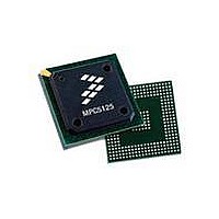
MPC5125YVN400 Freescale Semiconductor, MPC5125YVN400 Datasheet - Page 175

MPC5125YVN400
Manufacturer Part Number
MPC5125YVN400
Description
IC MCU 32BIT E300 324TEPBGA
Manufacturer
Freescale Semiconductor
Series
MPC51xxr
Datasheets
1.MPC5125YVN400.pdf
(92 pages)
2.MPC5125YVN400.pdf
(8 pages)
3.MPC5125YVN400.pdf
(2 pages)
4.MPC5125YVN400.pdf
(1064 pages)
Specifications of MPC5125YVN400
Core Processor
e300
Core Size
32-Bit
Speed
400MHz
Connectivity
CAN, EBI/EMI, Ethernet, I²C, USB OTG
Peripherals
DMA, WDT
Number Of I /o
64
Program Memory Type
ROMless
Ram Size
32K x 8
Voltage - Supply (vcc/vdd)
1.33 V ~ 1.47 V
Oscillator Type
External
Operating Temperature
-40°C ~ 125°C
Package / Case
324-PBGA
Processor Series
MPC51xx
Core
e300
Data Bus Width
32 bit
Development Tools By Supplier
TWR-MPC5125-KIT, TWR-SER, TWR-ELEV, TOWER
Maximum Clock Frequency
400 MHz
Operating Supply Voltage
1.4 V
Maximum Operating Temperature
+ 125 C
Mounting Style
SMD/SMT
Data Ram Size
32 KB
I/o Voltage
3.3 V
Interface Type
CAN, I2C
Minimum Operating Temperature
- 40 C
Program Memory Size
32 bit
Cpu Speed
400MHz
Embedded Interface Type
CAN, I2C, SPI, UART, USB
Digital Ic Case Style
TEPBGA
No. Of Pins
324
Rohs Compliant
Yes
Cpu Family
MPC5xx
Device Core Size
32b
Frequency (max)
400MHz
Total Internal Ram Size
32KB
Instruction Set Architecture
RISC
Operating Temp Range
-40C to 85C
Operating Temperature Classification
Industrial
Mounting
Surface Mount
Pin Count
324
Lead Free Status / RoHS Status
Lead free / RoHS Compliant
Eeprom Size
-
Program Memory Size
-
Data Converters
-
Lead Free Status / Rohs Status
Lead free / RoHS Compliant
Available stocks
Company
Part Number
Manufacturer
Quantity
Price
Company:
Part Number:
MPC5125YVN400
Manufacturer:
Freescale Semiconductor
Quantity:
135
Company:
Part Number:
MPC5125YVN400
Manufacturer:
LTC
Quantity:
29
Company:
Part Number:
MPC5125YVN400
Manufacturer:
Freescale Semiconductor
Quantity:
10 000
- MPC5125YVN400 PDF datasheet
- MPC5125YVN400 PDF datasheet #2
- MPC5125YVN400 PDF datasheet #3
- MPC5125YVN400 PDF datasheet #4
- Current page: 175 of 1064
- Download datasheet (6Mb)
6.4.5.2
While this is the basic transmit flow, at times the message transmit process is interrupted. This can be due
to a loss of arbitration to a higher priority message or due to an error being detected on the network. For
the transmit routine, either of these events can be dealt with in a similar manner.
Freescale Semiconductor
2. When TDRE is indicated, write the next byte into the BDLC data register.
3. Write the last byte to the BDLC data register and set TEOD.
When a TDRE state is reflected in the BDLC_DLCBSVR register, the CPU writes the next byte to
be transmitted into the BDLC Data Register. This step is repeated until the last byte to be
transmitted is written to the BDLC Data Register.
After the user has written the last byte to be transmitted into the BDLC Data Register, the user then
sets the TEOD bit in BDLC Control Register 2. When the TEOD bit is set, once the byte written
to the BDLC Data Register is transmitted onto the bus, the BDLC module begins transmitting the
8-bit CRC byte, as specified in SAE J1850. Following the CRC byte, the BDLC module transmits
an EOD symbol onto the SAE J1850 bus, indicating that this part of the message has been
completed. If no IFR bytes are transmitted following the EOD, an EOF is recognized and the
message is complete.
Setting the TEOD bit is the last step the CPU needs to take to complete the message transmission,
and no further transmission-related interrupts occur. After the message has been completely
received by the BDLC module, an EOF interrupt is generated. However, this is technically a
receive function that can be managed by the message reception routine.
Transmitting Exceptions
If the user writes the first byte of a message to be transmitted to the BDLC
Data Register and then determines that a different message should be
transmitted, the user can write a new byte to the BDLC Data Register up
until the transmission begins. This new byte replaces the original byte in the
BDLC Data Register.
Due to the design and operation of the BDLC module, when transmitting a
message the user may write two, or possibly even three of the bytes to be
transmitted into the BDLC Data Register before the first RDRF interrupt
occurs. For this reason, the user should never use receive interrupts to
control the sequencing of bytes to be transmitted.
While the TEOD bit is typically set immediately following the write of the
last byte to the BDLC Data Register, it is also acceptable to wait until a
TDRE interrupt is generated before setting the TEOD bit. While the
example flowchart in
write to the BDLC Data Register, either method is correct. If a TDRE
interrupt is pending, it is cleared when the TEOD bit is set.
MPC5125 Microcontroller Reference Manual, Rev. 2
Figure 6-20
NOTE
NOTE
NOTE
shows the TEOD bit being set after the
Byte Data Link Controller (BDLC)
6-39
Related parts for MPC5125YVN400
Image
Part Number
Description
Manufacturer
Datasheet
Request
R
Part Number:
Description:
Mpc5125 Microcontroller Data Sheet
Manufacturer:
Freescale Semiconductor, Inc
Datasheet:

Part Number:
Description:
MPC5125 Microcontroller Data Sheet
Manufacturer:
FREESCALE [Freescale Semiconductor, Inc]
Datasheet:
Part Number:
Description:
Manufacturer:
Freescale Semiconductor, Inc
Datasheet:
Part Number:
Description:
Manufacturer:
Freescale Semiconductor, Inc
Datasheet:
Part Number:
Description:
Manufacturer:
Freescale Semiconductor, Inc
Datasheet:
Part Number:
Description:
Manufacturer:
Freescale Semiconductor, Inc
Datasheet:
Part Number:
Description:
Manufacturer:
Freescale Semiconductor, Inc
Datasheet:
Part Number:
Description:
Manufacturer:
Freescale Semiconductor, Inc
Datasheet:
Part Number:
Description:
Manufacturer:
Freescale Semiconductor, Inc
Datasheet:
Part Number:
Description:
Manufacturer:
Freescale Semiconductor, Inc
Datasheet:
Part Number:
Description:
Manufacturer:
Freescale Semiconductor, Inc
Datasheet:
Part Number:
Description:
Manufacturer:
Freescale Semiconductor, Inc
Datasheet:
Part Number:
Description:
Manufacturer:
Freescale Semiconductor, Inc
Datasheet:
Part Number:
Description:
Manufacturer:
Freescale Semiconductor, Inc
Datasheet:
Part Number:
Description:
Manufacturer:
Freescale Semiconductor, Inc
Datasheet:


