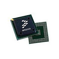
MPC5125YVN400 Freescale Semiconductor, MPC5125YVN400 Datasheet - Page 178

MPC5125YVN400
Manufacturer Part Number
MPC5125YVN400
Description
IC MCU 32BIT E300 324TEPBGA
Manufacturer
Freescale Semiconductor
Series
MPC51xxr
Datasheets
1.MPC5125YVN400.pdf
(92 pages)
2.MPC5125YVN400.pdf
(8 pages)
3.MPC5125YVN400.pdf
(2 pages)
4.MPC5125YVN400.pdf
(1064 pages)
Specifications of MPC5125YVN400
Core Processor
e300
Core Size
32-Bit
Speed
400MHz
Connectivity
CAN, EBI/EMI, Ethernet, I²C, USB OTG
Peripherals
DMA, WDT
Number Of I /o
64
Program Memory Type
ROMless
Ram Size
32K x 8
Voltage - Supply (vcc/vdd)
1.33 V ~ 1.47 V
Oscillator Type
External
Operating Temperature
-40°C ~ 125°C
Package / Case
324-PBGA
Processor Series
MPC51xx
Core
e300
Data Bus Width
32 bit
Development Tools By Supplier
TWR-MPC5125-KIT, TWR-SER, TWR-ELEV, TOWER
Maximum Clock Frequency
400 MHz
Operating Supply Voltage
1.4 V
Maximum Operating Temperature
+ 125 C
Mounting Style
SMD/SMT
Data Ram Size
32 KB
I/o Voltage
3.3 V
Interface Type
CAN, I2C
Minimum Operating Temperature
- 40 C
Program Memory Size
32 bit
Cpu Speed
400MHz
Embedded Interface Type
CAN, I2C, SPI, UART, USB
Digital Ic Case Style
TEPBGA
No. Of Pins
324
Rohs Compliant
Yes
Cpu Family
MPC5xx
Device Core Size
32b
Frequency (max)
400MHz
Total Internal Ram Size
32KB
Instruction Set Architecture
RISC
Operating Temp Range
-40C to 85C
Operating Temperature Classification
Industrial
Mounting
Surface Mount
Pin Count
324
Lead Free Status / RoHS Status
Lead free / RoHS Compliant
Eeprom Size
-
Program Memory Size
-
Data Converters
-
Lead Free Status / Rohs Status
Lead free / RoHS Compliant
Available stocks
Company
Part Number
Manufacturer
Quantity
Price
Company:
Part Number:
MPC5125YVN400
Manufacturer:
Freescale Semiconductor
Quantity:
135
Company:
Part Number:
MPC5125YVN400
Manufacturer:
LTC
Quantity:
29
Company:
Part Number:
MPC5125YVN400
Manufacturer:
Freescale Semiconductor
Quantity:
10 000
- MPC5125YVN400 PDF datasheet
- MPC5125YVN400 PDF datasheet #2
- MPC5125YVN400 PDF datasheet #3
- MPC5125YVN400 PDF datasheet #4
- Current page: 178 of 1064
- Download datasheet (6Mb)
Byte Data Link Controller (BDLC)
6.4.5.3
The BDLC module does not have a mechanism designed specifically for aborting a transmission. Because
the module transmits each message on a byte-by-byte basis, there is little need to implement an abort
mechanism. If the user has loaded a byte into the BDLC Data Register to initiate a message transmission
and decides to send a different message, the byte in the BDLC Data Register can be replaced, right up to
the point that the message transmission begins.
If the user has loaded a byte into the BDLC Data Register and then decides not to send any message at all,
the user can let the byte transmit, and when the TDRE interrupt occurs let the transmitter underrun. This
causes two extra logic ones followed by an EOF to be transmitted. While this method may require a small
amount of bus bandwidth, the need to do this should be rare. Replacing the byte originally written to the
BDLC Data Register with 0xFF also increases the probability of the transmitter losing arbitration if
another node begins transmitting at the same time, also reducing the bus bandwidth needed.
6.4.6
The design of the BDLC module makes it especially easy to use for receiving messages off of the SAE
J1850 bus. When the first byte of a message comes in, the BDLC_DLCBSVR register indicates to the CPU
that a byte has been received. As each successive byte is received, it is in turn be reflected in the
BDLC_DLCBSVR register. When the message is complete and the EOF has been detected on the bus, the
BDLC_DLCBSVR register reflects this, indicating that the message is complete.
The basic steps required for receiving a message from the SAE J1850 bus are outlined below. For more
information on receiving IFR bytes, refer to
6.4.6.1
The only control bit used for message reception, the IMSG bit, is actually used to prevent message
reception. When the IMSG bit is set, some of the BDLC module interrupts of the CPU are inhibited until
the next SOF symbol is received. This allows the BDLC module to ignore the remainder of a message once
the CPU has determined that it is of no interest. This helps reduce the amount of CPU overhead used to
service messages received from the SAE J1850 network, since otherwise the BDLC module would require
attention from the CPU for each byte broadcast on the network. The IMSG bit is cleared when the BDLC
module receives an SOF symbol, or it can also be cleared by the CPU.
6-42
Receiving A Message
Aborting a Transmission
BDLC Reception Control Bits
While the IMSG bit can be used to prevent the CPU from having to service
the BDLC module for every byte transmitted on the SAE J1850 bus, the
IMSG bit should never be used to ignore the BDLC module’s own
transmission. Because setting the IMSG bit prevents some
BDLC_DLCBSVR register bits from being updated, it may be difficult for
the CPU to complete the transmission correctly.
MPC5125 Microcontroller Reference Manual, Rev. 2
Section 6.4.8, “Receiving An In-Frame Response (IFR).”
NOTE
Freescale Semiconductor
Related parts for MPC5125YVN400
Image
Part Number
Description
Manufacturer
Datasheet
Request
R
Part Number:
Description:
Mpc5125 Microcontroller Data Sheet
Manufacturer:
Freescale Semiconductor, Inc
Datasheet:

Part Number:
Description:
MPC5125 Microcontroller Data Sheet
Manufacturer:
FREESCALE [Freescale Semiconductor, Inc]
Datasheet:
Part Number:
Description:
Manufacturer:
Freescale Semiconductor, Inc
Datasheet:
Part Number:
Description:
Manufacturer:
Freescale Semiconductor, Inc
Datasheet:
Part Number:
Description:
Manufacturer:
Freescale Semiconductor, Inc
Datasheet:
Part Number:
Description:
Manufacturer:
Freescale Semiconductor, Inc
Datasheet:
Part Number:
Description:
Manufacturer:
Freescale Semiconductor, Inc
Datasheet:
Part Number:
Description:
Manufacturer:
Freescale Semiconductor, Inc
Datasheet:
Part Number:
Description:
Manufacturer:
Freescale Semiconductor, Inc
Datasheet:
Part Number:
Description:
Manufacturer:
Freescale Semiconductor, Inc
Datasheet:
Part Number:
Description:
Manufacturer:
Freescale Semiconductor, Inc
Datasheet:
Part Number:
Description:
Manufacturer:
Freescale Semiconductor, Inc
Datasheet:
Part Number:
Description:
Manufacturer:
Freescale Semiconductor, Inc
Datasheet:
Part Number:
Description:
Manufacturer:
Freescale Semiconductor, Inc
Datasheet:
Part Number:
Description:
Manufacturer:
Freescale Semiconductor, Inc
Datasheet:


