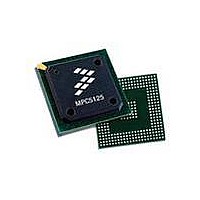
MPC5125YVN400 Freescale Semiconductor, MPC5125YVN400 Datasheet - Page 157

MPC5125YVN400
Manufacturer Part Number
MPC5125YVN400
Description
IC MCU 32BIT E300 324TEPBGA
Manufacturer
Freescale Semiconductor
Series
MPC51xxr
Datasheets
1.MPC5125YVN400.pdf
(92 pages)
2.MPC5125YVN400.pdf
(8 pages)
3.MPC5125YVN400.pdf
(2 pages)
4.MPC5125YVN400.pdf
(1064 pages)
Specifications of MPC5125YVN400
Core Processor
e300
Core Size
32-Bit
Speed
400MHz
Connectivity
CAN, EBI/EMI, Ethernet, I²C, USB OTG
Peripherals
DMA, WDT
Number Of I /o
64
Program Memory Type
ROMless
Ram Size
32K x 8
Voltage - Supply (vcc/vdd)
1.33 V ~ 1.47 V
Oscillator Type
External
Operating Temperature
-40°C ~ 125°C
Package / Case
324-PBGA
Processor Series
MPC51xx
Core
e300
Data Bus Width
32 bit
Development Tools By Supplier
TWR-MPC5125-KIT, TWR-SER, TWR-ELEV, TOWER
Maximum Clock Frequency
400 MHz
Operating Supply Voltage
1.4 V
Maximum Operating Temperature
+ 125 C
Mounting Style
SMD/SMT
Data Ram Size
32 KB
I/o Voltage
3.3 V
Interface Type
CAN, I2C
Minimum Operating Temperature
- 40 C
Program Memory Size
32 bit
Cpu Speed
400MHz
Embedded Interface Type
CAN, I2C, SPI, UART, USB
Digital Ic Case Style
TEPBGA
No. Of Pins
324
Rohs Compliant
Yes
Cpu Family
MPC5xx
Device Core Size
32b
Frequency (max)
400MHz
Total Internal Ram Size
32KB
Instruction Set Architecture
RISC
Operating Temp Range
-40C to 85C
Operating Temperature Classification
Industrial
Mounting
Surface Mount
Pin Count
324
Lead Free Status / RoHS Status
Lead free / RoHS Compliant
Eeprom Size
-
Program Memory Size
-
Data Converters
-
Lead Free Status / Rohs Status
Lead free / RoHS Compliant
Available stocks
Company
Part Number
Manufacturer
Quantity
Price
Company:
Part Number:
MPC5125YVN400
Manufacturer:
Freescale Semiconductor
Quantity:
135
Company:
Part Number:
MPC5125YVN400
Manufacturer:
LTC
Quantity:
29
Company:
Part Number:
MPC5125YVN400
Manufacturer:
Freescale Semiconductor
Quantity:
10 000
- MPC5125YVN400 PDF datasheet
- MPC5125YVN400 PDF datasheet #2
- MPC5125YVN400 PDF datasheet #3
- MPC5125YVN400 PDF datasheet #4
- Current page: 157 of 1064
- Download datasheet (6Mb)
6.4.1.7
The IFS symbol is a passive period on the J1850 bus that allows proper synchronization between nodes
during continuous message transmission. The IFS symbol is transmitted by a node following the
completion of the EOF period.
When the last byte of a message has been transmitted onto the J1850 bus, and the EOF symbol time has
expired, all nodes must then wait for the IFS symbol time to expire before transmitting an SOF, marking
the beginning of another message.
However, if the BDLC module is waiting for the IFS period to expire before beginning a transmission and
a rising edge is detected before the IFS time has expired, it internally synchronizes to that edge.
A rising edge may occur during the IFS period because of varying clock tolerances and loading of the
J1850 bus, causing different nodes to observe the completion of the IFS period at different times. Receivers
must synchronize to any SOF occurring during an IFS period to allow for individual clock tolerances.
6.4.1.8
If the BDLC module is transmitting at the time a BREAK is detected, it treats the BREAK as if a
transmission error had occurred, and halts transmission.The BDLC module can transmit a BREAK
symbol. If while receiving a message the BDLC module detects a BREAK symbol, it treats the BREAK
as a reception error and sets the invalid symbol flag. If while receiving a message in 4X mode, the BDLC
module detects a BREAK symbol, it treats the BREAK as a reception error, sets BDLC_DLCBSVR
register to 0x1C, and exits 4X mode.The 4XE bit in BDLC Control Register 2 is automatically cleared
upon reception of the BREAK symbol.
6.4.1.9
An idle condition exists on the bus during any passive period after expiration of the IFS period. Any node
sensing an idle bus condition can begin transmission immediately.
6.4.2
Variable pulse width modulation (VPW) is an encoding technique in which each bit is defined by the time
between successive transitions, and by the level of the bus between transitions, active or passive. Active
and passive bits are used alternately. This encoding technique is used to reduced the number of bus
transitions for a given bit rate. See
The symbol values shown below are nominal values. Refer to the electrical specification for a more
complete description of symbol values. Each logic one or logic zero contains a single transition, and can
be at either the active or passive level and one of two lengths, either 64 µs or 128 µs (T
baud rate), depending upon the encoding of the previous bit. The SOF, EOD, EOF and IFS symbols are
always encoded at an assigned level and length. See
Each message begins with an SOF symbol, an active symbol. Therefore, each data byte (including the CRC
byte) begins with a passive bit, regardless of whether it is a logic 1 or a logic 0. All VPW bit lengths stated
in the following descriptions are typical values at a 10.4 kbit/s bit rate.
Freescale Semiconductor
J1850 VPW Symbols
Inter-Frame Separation Symbol (IFS)
Break
Idle Bus
MPC5125 Microcontroller Reference Manual, Rev. 2
Section 6.1.1, “Features.”
Figure
6-12.
Byte Data Link Controller (BDLC)
NOM
at 10.4 kbit/s
6-21
Related parts for MPC5125YVN400
Image
Part Number
Description
Manufacturer
Datasheet
Request
R
Part Number:
Description:
Mpc5125 Microcontroller Data Sheet
Manufacturer:
Freescale Semiconductor, Inc
Datasheet:

Part Number:
Description:
MPC5125 Microcontroller Data Sheet
Manufacturer:
FREESCALE [Freescale Semiconductor, Inc]
Datasheet:
Part Number:
Description:
Manufacturer:
Freescale Semiconductor, Inc
Datasheet:
Part Number:
Description:
Manufacturer:
Freescale Semiconductor, Inc
Datasheet:
Part Number:
Description:
Manufacturer:
Freescale Semiconductor, Inc
Datasheet:
Part Number:
Description:
Manufacturer:
Freescale Semiconductor, Inc
Datasheet:
Part Number:
Description:
Manufacturer:
Freescale Semiconductor, Inc
Datasheet:
Part Number:
Description:
Manufacturer:
Freescale Semiconductor, Inc
Datasheet:
Part Number:
Description:
Manufacturer:
Freescale Semiconductor, Inc
Datasheet:
Part Number:
Description:
Manufacturer:
Freescale Semiconductor, Inc
Datasheet:
Part Number:
Description:
Manufacturer:
Freescale Semiconductor, Inc
Datasheet:
Part Number:
Description:
Manufacturer:
Freescale Semiconductor, Inc
Datasheet:
Part Number:
Description:
Manufacturer:
Freescale Semiconductor, Inc
Datasheet:
Part Number:
Description:
Manufacturer:
Freescale Semiconductor, Inc
Datasheet:
Part Number:
Description:
Manufacturer:
Freescale Semiconductor, Inc
Datasheet:


