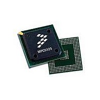
MPC5125YVN400 Freescale Semiconductor, MPC5125YVN400 Datasheet - Page 330

MPC5125YVN400
Manufacturer Part Number
MPC5125YVN400
Description
IC MCU 32BIT E300 324TEPBGA
Manufacturer
Freescale Semiconductor
Series
MPC51xxr
Datasheets
1.MPC5125YVN400.pdf
(92 pages)
2.MPC5125YVN400.pdf
(8 pages)
3.MPC5125YVN400.pdf
(2 pages)
4.MPC5125YVN400.pdf
(1064 pages)
Specifications of MPC5125YVN400
Core Processor
e300
Core Size
32-Bit
Speed
400MHz
Connectivity
CAN, EBI/EMI, Ethernet, I²C, USB OTG
Peripherals
DMA, WDT
Number Of I /o
64
Program Memory Type
ROMless
Ram Size
32K x 8
Voltage - Supply (vcc/vdd)
1.33 V ~ 1.47 V
Oscillator Type
External
Operating Temperature
-40°C ~ 125°C
Package / Case
324-PBGA
Processor Series
MPC51xx
Core
e300
Data Bus Width
32 bit
Development Tools By Supplier
TWR-MPC5125-KIT, TWR-SER, TWR-ELEV, TOWER
Maximum Clock Frequency
400 MHz
Operating Supply Voltage
1.4 V
Maximum Operating Temperature
+ 125 C
Mounting Style
SMD/SMT
Data Ram Size
32 KB
I/o Voltage
3.3 V
Interface Type
CAN, I2C
Minimum Operating Temperature
- 40 C
Program Memory Size
32 bit
Cpu Speed
400MHz
Embedded Interface Type
CAN, I2C, SPI, UART, USB
Digital Ic Case Style
TEPBGA
No. Of Pins
324
Rohs Compliant
Yes
Cpu Family
MPC5xx
Device Core Size
32b
Frequency (max)
400MHz
Total Internal Ram Size
32KB
Instruction Set Architecture
RISC
Operating Temp Range
-40C to 85C
Operating Temperature Classification
Industrial
Mounting
Surface Mount
Pin Count
324
Lead Free Status / RoHS Status
Lead free / RoHS Compliant
Eeprom Size
-
Program Memory Size
-
Data Converters
-
Lead Free Status / Rohs Status
Lead free / RoHS Compliant
Available stocks
Company
Part Number
Manufacturer
Quantity
Price
Company:
Part Number:
MPC5125YVN400
Manufacturer:
Freescale Semiconductor
Quantity:
135
Company:
Part Number:
MPC5125YVN400
Manufacturer:
LTC
Quantity:
29
Company:
Part Number:
MPC5125YVN400
Manufacturer:
Freescale Semiconductor
Quantity:
10 000
- MPC5125YVN400 PDF datasheet
- MPC5125YVN400 PDF datasheet #2
- MPC5125YVN400 PDF datasheet #3
- MPC5125YVN400 PDF datasheet #4
- Current page: 330 of 1064
- Download datasheet (6Mb)
DRAM Controller
The logic keeping track of what is currently possible on each of the banks is not in the DRAM command
engine. It is part of the timing manager, whose task is to signal to the DRAM command engine that
commands are currently possible.
11.4.4
All incoming writes are sent first to the write buffer, part of the command engine. Writes are sent to the
DRAM in background, whenever possible. The DRAM tries to postpone the writes until there are no
further outstanding read requests. However, when the write buffer is full, or when there is a new request
for an address already inside the write buffer, the DRAM controller writes the content of the write buffer
to the DRAM.
11.4.5
The timing manager consists of a bank of counters. These counters keeps track of all DRAM timing
parameters and signals to the DRAM command engine when a precharge, activate, read or write command
is possible. This information is supplied to the DRAM command engine for each bank separately.
All timing parameters are programmable in software.
11.4.6
Sending a read or write command to the DRAM is a two-step process. First, the command is sent, which
is done by the command engine. After some clock cycles, the data must follow.
Manipulating the read data is done by the read block. For every read command sent to the DRAM, the
command engine informs the read block. Upon receiving the read command, the read block delays this to
account for DRAM pipelining. Then, it receives the correct amount of data from the DRAM DQ inputs
and forwards this data to the correct bus.
Manipulating the write data is done by the write block. It works the same way as the read block. The
command engine informs the write block of a pending write. Upon receiving the command, the write block
delays this to account for DRAM pipelining. Then, it receives the relevant data from the write buffer and
transmits this to the DRAM.
11.4.7
The bus interface accepts a slave peripheral bus. The bus interface fulfills several functions:
11-22
•
•
•
For each bank, if the DRAM currently can accept a write command to it
It contains all configuration registers
It contains logic to send an error interrupt to the processor. The error interrupt is active when the
FIFO overflow or FIFO underflow error condition and corresponding interrupt enable in register
DDR_SYS_CONFIG is set. The register summary is given in
The FIFO overflow and underflow flags are tied to a FIFO that keeps track of the number of DQS
strobes the DRAM is expected to produce. If a read command is sent to the DRAM, the DRAM is
expected to answer after producing the read data on its DQ outputs, with some edges on its DQS
Write Buffer
Timing Manager
DRAM Read Block and DRAM Write Block
Bus Interface
MPC5125 Microcontroller Reference Manual, Rev. 2
Table
11-1.
Freescale Semiconductor
Related parts for MPC5125YVN400
Image
Part Number
Description
Manufacturer
Datasheet
Request
R
Part Number:
Description:
Mpc5125 Microcontroller Data Sheet
Manufacturer:
Freescale Semiconductor, Inc
Datasheet:

Part Number:
Description:
MPC5125 Microcontroller Data Sheet
Manufacturer:
FREESCALE [Freescale Semiconductor, Inc]
Datasheet:
Part Number:
Description:
Manufacturer:
Freescale Semiconductor, Inc
Datasheet:
Part Number:
Description:
Manufacturer:
Freescale Semiconductor, Inc
Datasheet:
Part Number:
Description:
Manufacturer:
Freescale Semiconductor, Inc
Datasheet:
Part Number:
Description:
Manufacturer:
Freescale Semiconductor, Inc
Datasheet:
Part Number:
Description:
Manufacturer:
Freescale Semiconductor, Inc
Datasheet:
Part Number:
Description:
Manufacturer:
Freescale Semiconductor, Inc
Datasheet:
Part Number:
Description:
Manufacturer:
Freescale Semiconductor, Inc
Datasheet:
Part Number:
Description:
Manufacturer:
Freescale Semiconductor, Inc
Datasheet:
Part Number:
Description:
Manufacturer:
Freescale Semiconductor, Inc
Datasheet:
Part Number:
Description:
Manufacturer:
Freescale Semiconductor, Inc
Datasheet:
Part Number:
Description:
Manufacturer:
Freescale Semiconductor, Inc
Datasheet:
Part Number:
Description:
Manufacturer:
Freescale Semiconductor, Inc
Datasheet:
Part Number:
Description:
Manufacturer:
Freescale Semiconductor, Inc
Datasheet:


