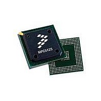
MPC5125YVN400 Freescale Semiconductor, MPC5125YVN400 Datasheet - Page 581

MPC5125YVN400
Manufacturer Part Number
MPC5125YVN400
Description
IC MCU 32BIT E300 324TEPBGA
Manufacturer
Freescale Semiconductor
Series
MPC51xxr
Datasheets
1.MPC5125YVN400.pdf
(92 pages)
2.MPC5125YVN400.pdf
(8 pages)
3.MPC5125YVN400.pdf
(2 pages)
4.MPC5125YVN400.pdf
(1064 pages)
Specifications of MPC5125YVN400
Core Processor
e300
Core Size
32-Bit
Speed
400MHz
Connectivity
CAN, EBI/EMI, Ethernet, I²C, USB OTG
Peripherals
DMA, WDT
Number Of I /o
64
Program Memory Type
ROMless
Ram Size
32K x 8
Voltage - Supply (vcc/vdd)
1.33 V ~ 1.47 V
Oscillator Type
External
Operating Temperature
-40°C ~ 125°C
Package / Case
324-PBGA
Processor Series
MPC51xx
Core
e300
Data Bus Width
32 bit
Development Tools By Supplier
TWR-MPC5125-KIT, TWR-SER, TWR-ELEV, TOWER
Maximum Clock Frequency
400 MHz
Operating Supply Voltage
1.4 V
Maximum Operating Temperature
+ 125 C
Mounting Style
SMD/SMT
Data Ram Size
32 KB
I/o Voltage
3.3 V
Interface Type
CAN, I2C
Minimum Operating Temperature
- 40 C
Program Memory Size
32 bit
Cpu Speed
400MHz
Embedded Interface Type
CAN, I2C, SPI, UART, USB
Digital Ic Case Style
TEPBGA
No. Of Pins
324
Rohs Compliant
Yes
Cpu Family
MPC5xx
Device Core Size
32b
Frequency (max)
400MHz
Total Internal Ram Size
32KB
Instruction Set Architecture
RISC
Operating Temp Range
-40C to 85C
Operating Temperature Classification
Industrial
Mounting
Surface Mount
Pin Count
324
Lead Free Status / RoHS Status
Lead free / RoHS Compliant
Eeprom Size
-
Program Memory Size
-
Data Converters
-
Lead Free Status / Rohs Status
Lead free / RoHS Compliant
Available stocks
Company
Part Number
Manufacturer
Quantity
Price
Company:
Part Number:
MPC5125YVN400
Manufacturer:
Freescale Semiconductor
Quantity:
135
Company:
Part Number:
MPC5125YVN400
Manufacturer:
LTC
Quantity:
29
Company:
Part Number:
MPC5125YVN400
Manufacturer:
Freescale Semiconductor
Quantity:
10 000
- MPC5125YVN400 PDF datasheet
- MPC5125YVN400 PDF datasheet #2
- MPC5125YVN400 PDF datasheet #3
- MPC5125YVN400 PDF datasheet #4
- Current page: 581 of 1064
- Download datasheet (6Mb)
22.2.1
CAN1_RX, CAN2_RX, DIU_LD00, I2C1_SCL, and DIU_LD08 are the MSCAN receiver input pins.
MSCAN3 can be configured to select DIU_LD00 or I2C1_SCL as input pin.
22.2.2
CAN1_TX, CAN2_TX, DIU_LD01, I2C1_SDA, and DIU_LD09 are MSCAN transmitter output pins.
MSCAN3 can be configured to select DIU_LD01 or I2C1_SDA as output pin. These pins represents the
logic level on the CAN bus:
22.2.3
A typical CAN system with MSCAN is shown in
to the CAN bus lines through a transceiver device. The transceiver is capable of driving the large current
needed for the CAN bus and has current protection against defective CAN or defective stations.
Freescale Semiconductor
DIU_LD00/
DIU_LD01/
CAN1_TX/
CAN2_TX/
I2C1_SDA
CAN1_RX
CAN2_RX
I2C1_SCL
DIU_LD08
DIU_LD09
PSC0_4
PSC1_0
Name
0 = Dominant state
1 = Recessive state
CAN Receiver Input Pins
CAN Transmitter Output Pins
CAN System
Output MSCAN1 transmitter output pin. The CAN1_TX/PSC0_4 output pin represents the logic level on
Output MSCAN2 transmitter output pin. The CAN2_TX/PSC1_0 output pin represents the logic level on
Output MSCAN3 transmitter output pin. The DIU_LD01/I2C1_SDA output pin represents the logic level
Output MSCAN4 transmitter output pin. The DIU_LD09 output pin represents the logic level on the CAN
Input
Input
Input
Input
Port
MSCAN1 receiver input pin
the CAN bus:
0 Dominant state
1 Recessive state
MSCAN2 receiver input pin
the CAN bus:
0 Dominant state
1 Recessive state
MSCAN3 receiver input pin
on the CAN bus:
0 Dominant state
1 Recessive state
MSCAN4 receiver input pin
bus:
0 Dominant state
1 Recessive state
MPC5125 Microcontroller Reference Manual, Rev. 2
Table 22-1. Signal Properties
Figure
Function
22-2. Each CAN station is connected physically
MSCAN
22-3
I/O
O
O
O
O
I
I
I
I
Related parts for MPC5125YVN400
Image
Part Number
Description
Manufacturer
Datasheet
Request
R
Part Number:
Description:
Mpc5125 Microcontroller Data Sheet
Manufacturer:
Freescale Semiconductor, Inc
Datasheet:

Part Number:
Description:
MPC5125 Microcontroller Data Sheet
Manufacturer:
FREESCALE [Freescale Semiconductor, Inc]
Datasheet:
Part Number:
Description:
Manufacturer:
Freescale Semiconductor, Inc
Datasheet:
Part Number:
Description:
Manufacturer:
Freescale Semiconductor, Inc
Datasheet:
Part Number:
Description:
Manufacturer:
Freescale Semiconductor, Inc
Datasheet:
Part Number:
Description:
Manufacturer:
Freescale Semiconductor, Inc
Datasheet:
Part Number:
Description:
Manufacturer:
Freescale Semiconductor, Inc
Datasheet:
Part Number:
Description:
Manufacturer:
Freescale Semiconductor, Inc
Datasheet:
Part Number:
Description:
Manufacturer:
Freescale Semiconductor, Inc
Datasheet:
Part Number:
Description:
Manufacturer:
Freescale Semiconductor, Inc
Datasheet:
Part Number:
Description:
Manufacturer:
Freescale Semiconductor, Inc
Datasheet:
Part Number:
Description:
Manufacturer:
Freescale Semiconductor, Inc
Datasheet:
Part Number:
Description:
Manufacturer:
Freescale Semiconductor, Inc
Datasheet:
Part Number:
Description:
Manufacturer:
Freescale Semiconductor, Inc
Datasheet:
Part Number:
Description:
Manufacturer:
Freescale Semiconductor, Inc
Datasheet:


