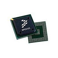
MPC5125YVN400 Freescale Semiconductor, MPC5125YVN400 Datasheet - Page 171

MPC5125YVN400
Manufacturer Part Number
MPC5125YVN400
Description
IC MCU 32BIT E300 324TEPBGA
Manufacturer
Freescale Semiconductor
Series
MPC51xxr
Datasheets
1.MPC5125YVN400.pdf
(92 pages)
2.MPC5125YVN400.pdf
(8 pages)
3.MPC5125YVN400.pdf
(2 pages)
4.MPC5125YVN400.pdf
(1064 pages)
Specifications of MPC5125YVN400
Core Processor
e300
Core Size
32-Bit
Speed
400MHz
Connectivity
CAN, EBI/EMI, Ethernet, I²C, USB OTG
Peripherals
DMA, WDT
Number Of I /o
64
Program Memory Type
ROMless
Ram Size
32K x 8
Voltage - Supply (vcc/vdd)
1.33 V ~ 1.47 V
Oscillator Type
External
Operating Temperature
-40°C ~ 125°C
Package / Case
324-PBGA
Processor Series
MPC51xx
Core
e300
Data Bus Width
32 bit
Development Tools By Supplier
TWR-MPC5125-KIT, TWR-SER, TWR-ELEV, TOWER
Maximum Clock Frequency
400 MHz
Operating Supply Voltage
1.4 V
Maximum Operating Temperature
+ 125 C
Mounting Style
SMD/SMT
Data Ram Size
32 KB
I/o Voltage
3.3 V
Interface Type
CAN, I2C
Minimum Operating Temperature
- 40 C
Program Memory Size
32 bit
Cpu Speed
400MHz
Embedded Interface Type
CAN, I2C, SPI, UART, USB
Digital Ic Case Style
TEPBGA
No. Of Pins
324
Rohs Compliant
Yes
Cpu Family
MPC5xx
Device Core Size
32b
Frequency (max)
400MHz
Total Internal Ram Size
32KB
Instruction Set Architecture
RISC
Operating Temp Range
-40C to 85C
Operating Temperature Classification
Industrial
Mounting
Surface Mount
Pin Count
324
Lead Free Status / RoHS Status
Lead free / RoHS Compliant
Eeprom Size
-
Program Memory Size
-
Data Converters
-
Lead Free Status / Rohs Status
Lead free / RoHS Compliant
Available stocks
Company
Part Number
Manufacturer
Quantity
Price
Company:
Part Number:
MPC5125YVN400
Manufacturer:
Freescale Semiconductor
Quantity:
135
Company:
Part Number:
MPC5125YVN400
Manufacturer:
LTC
Quantity:
29
Company:
Part Number:
MPC5125YVN400
Manufacturer:
Freescale Semiconductor
Quantity:
10 000
- MPC5125YVN400 PDF datasheet
- MPC5125YVN400 PDF datasheet #2
- MPC5125YVN400 PDF datasheet #3
- MPC5125YVN400 PDF datasheet #4
- Current page: 171 of 1064
- Download datasheet (6Mb)
transition occurs with respect to the sampling points. This filter delay must be taken into account when
performing message arbitration.
For example, if the frequency of the MUX Interface clock (f
954ns and the maximum filter delay in the absence of noise is 15.259 µs.
The effect of random noise on the J1850_RX signal depends on the characteristics of the noise itself.
Narrow noise pulses on the J1850_RX signal is completely ignored if they are shorter than the filter delay.
This provides a degree of low pass filtering.
If noise occurs during a symbol transition, the detection of that transition may be delayed by an amount
equal to the length of the noise burst. This is a reflection of the uncertainty of where the transition is truly
occurring within the noise.
Noise pulses that are wider than the filter delay, but narrower than the shortest allowable symbol length is
detected by the next stage of the BDLC module’s receiver as an invalid symbol.
Noise pulses that are longer than the shortest allowable symbol length is normally detected as an invalid
symbol or as invalid data when the frame’s CRC is checked.
6.4.4
The Protocol Handler is responsible for framing, collision detection, arbitration, CRC
generation/checking, and error detection. The Protocol Handler conforms to SAE J1850 - Class B Data
Communications Network Interface. Refer to
6.4.4.1
The Protocol Handler contains the State Machine, Rx Shadow Register, Tx Shadow Register, Rx Shift
Register, Tx Shift Register, and Loopback Multiplexer as shown in
6.4.4.1.1
The Rx Shift Register gathers received serial data bits from the J1850 bus and makes them available in
parallel form to the Rx Shadow Register. The Tx Shift Register takes data, in parallel form, from the Tx
Shadow Register and presents it serially to the State Machine so that it can be transmitted onto the J1850
bus.
Freescale Semiconductor
Protocol Handler
Protocol Architecture
Rx and Tx Shift Registers
MPC5125 Microcontroller Reference Manual, Rev. 2
Figure
6-1.
bdlc
) is 1.0486MHz, then the period (t
Figure
6-19.
Byte Data Link Controller (BDLC)
bdlc
) is
6-35
Related parts for MPC5125YVN400
Image
Part Number
Description
Manufacturer
Datasheet
Request
R
Part Number:
Description:
Mpc5125 Microcontroller Data Sheet
Manufacturer:
Freescale Semiconductor, Inc
Datasheet:

Part Number:
Description:
MPC5125 Microcontroller Data Sheet
Manufacturer:
FREESCALE [Freescale Semiconductor, Inc]
Datasheet:
Part Number:
Description:
Manufacturer:
Freescale Semiconductor, Inc
Datasheet:
Part Number:
Description:
Manufacturer:
Freescale Semiconductor, Inc
Datasheet:
Part Number:
Description:
Manufacturer:
Freescale Semiconductor, Inc
Datasheet:
Part Number:
Description:
Manufacturer:
Freescale Semiconductor, Inc
Datasheet:
Part Number:
Description:
Manufacturer:
Freescale Semiconductor, Inc
Datasheet:
Part Number:
Description:
Manufacturer:
Freescale Semiconductor, Inc
Datasheet:
Part Number:
Description:
Manufacturer:
Freescale Semiconductor, Inc
Datasheet:
Part Number:
Description:
Manufacturer:
Freescale Semiconductor, Inc
Datasheet:
Part Number:
Description:
Manufacturer:
Freescale Semiconductor, Inc
Datasheet:
Part Number:
Description:
Manufacturer:
Freescale Semiconductor, Inc
Datasheet:
Part Number:
Description:
Manufacturer:
Freescale Semiconductor, Inc
Datasheet:
Part Number:
Description:
Manufacturer:
Freescale Semiconductor, Inc
Datasheet:
Part Number:
Description:
Manufacturer:
Freescale Semiconductor, Inc
Datasheet:


