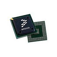
MPC5125YVN400 Freescale Semiconductor, MPC5125YVN400 Datasheet - Page 306

MPC5125YVN400
Manufacturer Part Number
MPC5125YVN400
Description
IC MCU 32BIT E300 324TEPBGA
Manufacturer
Freescale Semiconductor
Series
MPC51xxr
Datasheets
1.MPC5125YVN400.pdf
(92 pages)
2.MPC5125YVN400.pdf
(8 pages)
3.MPC5125YVN400.pdf
(2 pages)
4.MPC5125YVN400.pdf
(1064 pages)
Specifications of MPC5125YVN400
Core Processor
e300
Core Size
32-Bit
Speed
400MHz
Connectivity
CAN, EBI/EMI, Ethernet, I²C, USB OTG
Peripherals
DMA, WDT
Number Of I /o
64
Program Memory Type
ROMless
Ram Size
32K x 8
Voltage - Supply (vcc/vdd)
1.33 V ~ 1.47 V
Oscillator Type
External
Operating Temperature
-40°C ~ 125°C
Package / Case
324-PBGA
Processor Series
MPC51xx
Core
e300
Data Bus Width
32 bit
Development Tools By Supplier
TWR-MPC5125-KIT, TWR-SER, TWR-ELEV, TOWER
Maximum Clock Frequency
400 MHz
Operating Supply Voltage
1.4 V
Maximum Operating Temperature
+ 125 C
Mounting Style
SMD/SMT
Data Ram Size
32 KB
I/o Voltage
3.3 V
Interface Type
CAN, I2C
Minimum Operating Temperature
- 40 C
Program Memory Size
32 bit
Cpu Speed
400MHz
Embedded Interface Type
CAN, I2C, SPI, UART, USB
Digital Ic Case Style
TEPBGA
No. Of Pins
324
Rohs Compliant
Yes
Cpu Family
MPC5xx
Device Core Size
32b
Frequency (max)
400MHz
Total Internal Ram Size
32KB
Instruction Set Architecture
RISC
Operating Temp Range
-40C to 85C
Operating Temperature Classification
Industrial
Mounting
Surface Mount
Pin Count
324
Lead Free Status / RoHS Status
Lead free / RoHS Compliant
Eeprom Size
-
Program Memory Size
-
Data Converters
-
Lead Free Status / Rohs Status
Lead free / RoHS Compliant
Available stocks
Company
Part Number
Manufacturer
Quantity
Price
Company:
Part Number:
MPC5125YVN400
Manufacturer:
Freescale Semiconductor
Quantity:
135
Company:
Part Number:
MPC5125YVN400
Manufacturer:
LTC
Quantity:
29
Company:
Part Number:
MPC5125YVN400
Manufacturer:
Freescale Semiconductor
Quantity:
10 000
- MPC5125YVN400 PDF datasheet
- MPC5125YVN400 PDF datasheet #2
- MPC5125YVN400 PDF datasheet #3
- MPC5125YVN400 PDF datasheet #4
- Current page: 306 of 1064
- Download datasheet (6Mb)
Display Interface Unit (DIU)
By default, the DIU outputs (data and sync signals) switch at same time with the pixel clock rising edge.
To provide flexibility in meeting the timing requirements of different LCD display drivers, the user can
perform minor tuning of the timing of the pixel clock found on the DIU_CLK pin relative to all the other
DIU signals (DIU_LD[23:0], DIU_VSYNC, DIU_HSYNC, DIU_DE). This phase tuning is done using
programmable parameters in the DCCR register, specifically DCCR[CLK_INV] and DCCR[DLY_NUM]
(refer to
does not change the pixel clock frequency or duty cycle.
10.4.13.1 Refresh Rate
The refresh rate (or frame rate) is the number of times that the display is updated in a second. It can be
calculated from the timing parameters using this formula:
Because the user probably has a set target refresh rate (RR), the PIX_CLK value has been set already and
the DELTA_X and DELTA_Y values are determined exactly by the panel used. The rest of the parameters
in this equation must be chosen to approach the desired refresh rate while complying with the requirements
established in the panel’s data sheet for the front and back porches.
10.5
10.5.1
The procedure to bring up the DIU out of hardware reset state, start executing data processing, and display
functions is as follows:
10-44
1. Hardware reset.
2. Configure I/O function multiplexing and drive strength for DIU related pins.
3. Program the display timing signal generation related registers. Failing to set appropriate values for
the display timing parameters may result in damage to the display.
Chapter 5, “Clocks and Low-Power
Initialization/Application Information
DIU Initialization
rr
=
---------------------------------------------------------------------------------------------------------------------------------------------------------------------- -
(
delta_x
+
MPC5125 Microcontroller Reference Manual, Rev. 2
fp_h
Figure 10-50. Vertical Sync Signals
+
pw_h
+
Modes”). Phase tuning using CLK_INV and DLY_NUM
bp_h
pix_clk
)
×
(
delta_y
+
fp_v
+
pw_v
+
bp_v
Freescale Semiconductor
)
Eqn. 10-3
Related parts for MPC5125YVN400
Image
Part Number
Description
Manufacturer
Datasheet
Request
R
Part Number:
Description:
Mpc5125 Microcontroller Data Sheet
Manufacturer:
Freescale Semiconductor, Inc
Datasheet:

Part Number:
Description:
MPC5125 Microcontroller Data Sheet
Manufacturer:
FREESCALE [Freescale Semiconductor, Inc]
Datasheet:
Part Number:
Description:
Manufacturer:
Freescale Semiconductor, Inc
Datasheet:
Part Number:
Description:
Manufacturer:
Freescale Semiconductor, Inc
Datasheet:
Part Number:
Description:
Manufacturer:
Freescale Semiconductor, Inc
Datasheet:
Part Number:
Description:
Manufacturer:
Freescale Semiconductor, Inc
Datasheet:
Part Number:
Description:
Manufacturer:
Freescale Semiconductor, Inc
Datasheet:
Part Number:
Description:
Manufacturer:
Freescale Semiconductor, Inc
Datasheet:
Part Number:
Description:
Manufacturer:
Freescale Semiconductor, Inc
Datasheet:
Part Number:
Description:
Manufacturer:
Freescale Semiconductor, Inc
Datasheet:
Part Number:
Description:
Manufacturer:
Freescale Semiconductor, Inc
Datasheet:
Part Number:
Description:
Manufacturer:
Freescale Semiconductor, Inc
Datasheet:
Part Number:
Description:
Manufacturer:
Freescale Semiconductor, Inc
Datasheet:
Part Number:
Description:
Manufacturer:
Freescale Semiconductor, Inc
Datasheet:
Part Number:
Description:
Manufacturer:
Freescale Semiconductor, Inc
Datasheet:


