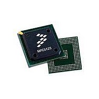
MPC5125YVN400 Freescale Semiconductor, MPC5125YVN400 Datasheet - Page 196

MPC5125YVN400
Manufacturer Part Number
MPC5125YVN400
Description
IC MCU 32BIT E300 324TEPBGA
Manufacturer
Freescale Semiconductor
Series
MPC51xxr
Datasheets
1.MPC5125YVN400.pdf
(92 pages)
2.MPC5125YVN400.pdf
(8 pages)
3.MPC5125YVN400.pdf
(2 pages)
4.MPC5125YVN400.pdf
(1064 pages)
Specifications of MPC5125YVN400
Core Processor
e300
Core Size
32-Bit
Speed
400MHz
Connectivity
CAN, EBI/EMI, Ethernet, I²C, USB OTG
Peripherals
DMA, WDT
Number Of I /o
64
Program Memory Type
ROMless
Ram Size
32K x 8
Voltage - Supply (vcc/vdd)
1.33 V ~ 1.47 V
Oscillator Type
External
Operating Temperature
-40°C ~ 125°C
Package / Case
324-PBGA
Processor Series
MPC51xx
Core
e300
Data Bus Width
32 bit
Development Tools By Supplier
TWR-MPC5125-KIT, TWR-SER, TWR-ELEV, TOWER
Maximum Clock Frequency
400 MHz
Operating Supply Voltage
1.4 V
Maximum Operating Temperature
+ 125 C
Mounting Style
SMD/SMT
Data Ram Size
32 KB
I/o Voltage
3.3 V
Interface Type
CAN, I2C
Minimum Operating Temperature
- 40 C
Program Memory Size
32 bit
Cpu Speed
400MHz
Embedded Interface Type
CAN, I2C, SPI, UART, USB
Digital Ic Case Style
TEPBGA
No. Of Pins
324
Rohs Compliant
Yes
Cpu Family
MPC5xx
Device Core Size
32b
Frequency (max)
400MHz
Total Internal Ram Size
32KB
Instruction Set Architecture
RISC
Operating Temp Range
-40C to 85C
Operating Temperature Classification
Industrial
Mounting
Surface Mount
Pin Count
324
Lead Free Status / RoHS Status
Lead free / RoHS Compliant
Eeprom Size
-
Program Memory Size
-
Data Converters
-
Lead Free Status / Rohs Status
Lead free / RoHS Compliant
Available stocks
Company
Part Number
Manufacturer
Quantity
Price
Company:
Part Number:
MPC5125YVN400
Manufacturer:
Freescale Semiconductor
Quantity:
135
Company:
Part Number:
MPC5125YVN400
Manufacturer:
LTC
Quantity:
29
Company:
Part Number:
MPC5125YVN400
Manufacturer:
Freescale Semiconductor
Quantity:
10 000
- MPC5125YVN400 PDF datasheet
- MPC5125YVN400 PDF datasheet #2
- MPC5125YVN400 PDF datasheet #3
- MPC5125YVN400 PDF datasheet #4
- Current page: 196 of 1064
- Download datasheet (6Mb)
Byte Data Link Controller (BDLC)
6.5.2
After the configuration bits have been written to the desired values, the BDLC module should be taken out
of loopback and connected to the SAE J1850 bus. This is done by clearing the DLOOP bit and then setting
the BDLCE bit in the BDLC Control Register.
After DLOOP is cleared and BDLCE is set, the BDLC module is ready for SAE J1850 communication.
However, to ensure that the BDLC module does not attempt to receive a message already in progress or to
transmit a message while another device is transmitting, the BDLC module must first observe an EOF
symbol on the bus before the receiver is activated. To activate the transmitter, the BDLC module needs to
observe an Inter-Frame Separator symbol.
6.5.3
The final step in readying the BDLC module for proper communication is to clear any pending interrupt
sources and then, if desired, enable BDLC module interrupts of the CPU.
6-60
4. Initialize the BDLC_DLCBCR1 register.
1. Perform Loopback Tests (optional)
2. Exit Loopback Mode and Enable the BDLC Module
1. Clear Pending BDLC Interrupts
The next step in BDLC module initialization should be writing the configuration bits into the
BDLC Control Register 2 register. This initialization description assumes the BDLC module is put
into normal mode (not 4X mode), and that the BDLC module should not yet exit digital or analog
loopback mode. Therefore, this step should write SMRST and DLOOP as logic ones, 4XE as a
logic zero, write NBFS to the desired level, and write TEOD, TSIFR, TMIFR1, and TMIFR0 as
logic zeros. These last four bits MUST be written as logic zeros to prevent undesired operation of
the BDLC module.
The next step in BDLC module initialization is to write the configuration bits in the
BDLC_DLCBCR1 register. The CLKS bit should be written to its desired values at this time,
following which it becomes read-only. The IE bit should be written as a logic zero at this time so
BDLC module interrupts of the CPU remain masked for the time being. The IMSG bit should be
written as a logic one to prevent any receive events from setting the BDLC_DLCBSVR register
until a valid SOF (or BREAK) symbol has been received by the BDLC module.
After the BDLC module is configured for desired operation, the user may wish to perform digital
and/or analog loopback tests to determine the integrity of the link to the SAE J1850 network. This
would involve leaving the DLOOP bit (BDLC Control Register 2) set, setting the BDLCE bit,
preforming the desired loopback tests and finally exiting digital loopback mode by clearing
DLOOP in the BDLC Control Register 2.
If loopback mode tests are not to be preformed the BDLC module can be removed from digital
loopback mode by clearing the DLOOP bit. The BDLC module can then be enabled by setting the
BDLCE bit in the BDLC Control Register.
To ensure that the BDLC module does not immediately generate a CPU interrupt when interrupts
are enabled, the user should read the BDLC_DLCBSVR register to determine if any BDLC module
Exiting Loopback Mode and Enabling the BDLC Module
Enabling BDLC Interrupts
MPC5125 Microcontroller Reference Manual, Rev. 2
Freescale Semiconductor
Related parts for MPC5125YVN400
Image
Part Number
Description
Manufacturer
Datasheet
Request
R
Part Number:
Description:
Mpc5125 Microcontroller Data Sheet
Manufacturer:
Freescale Semiconductor, Inc
Datasheet:

Part Number:
Description:
MPC5125 Microcontroller Data Sheet
Manufacturer:
FREESCALE [Freescale Semiconductor, Inc]
Datasheet:
Part Number:
Description:
Manufacturer:
Freescale Semiconductor, Inc
Datasheet:
Part Number:
Description:
Manufacturer:
Freescale Semiconductor, Inc
Datasheet:
Part Number:
Description:
Manufacturer:
Freescale Semiconductor, Inc
Datasheet:
Part Number:
Description:
Manufacturer:
Freescale Semiconductor, Inc
Datasheet:
Part Number:
Description:
Manufacturer:
Freescale Semiconductor, Inc
Datasheet:
Part Number:
Description:
Manufacturer:
Freescale Semiconductor, Inc
Datasheet:
Part Number:
Description:
Manufacturer:
Freescale Semiconductor, Inc
Datasheet:
Part Number:
Description:
Manufacturer:
Freescale Semiconductor, Inc
Datasheet:
Part Number:
Description:
Manufacturer:
Freescale Semiconductor, Inc
Datasheet:
Part Number:
Description:
Manufacturer:
Freescale Semiconductor, Inc
Datasheet:
Part Number:
Description:
Manufacturer:
Freescale Semiconductor, Inc
Datasheet:
Part Number:
Description:
Manufacturer:
Freescale Semiconductor, Inc
Datasheet:
Part Number:
Description:
Manufacturer:
Freescale Semiconductor, Inc
Datasheet:


