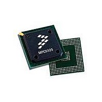
MPC5125YVN400 Freescale Semiconductor, MPC5125YVN400 Datasheet - Page 545

MPC5125YVN400
Manufacturer Part Number
MPC5125YVN400
Description
IC MCU 32BIT E300 324TEPBGA
Manufacturer
Freescale Semiconductor
Series
MPC51xxr
Datasheets
1.MPC5125YVN400.pdf
(92 pages)
2.MPC5125YVN400.pdf
(8 pages)
3.MPC5125YVN400.pdf
(2 pages)
4.MPC5125YVN400.pdf
(1064 pages)
Specifications of MPC5125YVN400
Core Processor
e300
Core Size
32-Bit
Speed
400MHz
Connectivity
CAN, EBI/EMI, Ethernet, I²C, USB OTG
Peripherals
DMA, WDT
Number Of I /o
64
Program Memory Type
ROMless
Ram Size
32K x 8
Voltage - Supply (vcc/vdd)
1.33 V ~ 1.47 V
Oscillator Type
External
Operating Temperature
-40°C ~ 125°C
Package / Case
324-PBGA
Processor Series
MPC51xx
Core
e300
Data Bus Width
32 bit
Development Tools By Supplier
TWR-MPC5125-KIT, TWR-SER, TWR-ELEV, TOWER
Maximum Clock Frequency
400 MHz
Operating Supply Voltage
1.4 V
Maximum Operating Temperature
+ 125 C
Mounting Style
SMD/SMT
Data Ram Size
32 KB
I/o Voltage
3.3 V
Interface Type
CAN, I2C
Minimum Operating Temperature
- 40 C
Program Memory Size
32 bit
Cpu Speed
400MHz
Embedded Interface Type
CAN, I2C, SPI, UART, USB
Digital Ic Case Style
TEPBGA
No. Of Pins
324
Rohs Compliant
Yes
Cpu Family
MPC5xx
Device Core Size
32b
Frequency (max)
400MHz
Total Internal Ram Size
32KB
Instruction Set Architecture
RISC
Operating Temp Range
-40C to 85C
Operating Temperature Classification
Industrial
Mounting
Surface Mount
Pin Count
324
Lead Free Status / RoHS Status
Lead free / RoHS Compliant
Eeprom Size
-
Program Memory Size
-
Data Converters
-
Lead Free Status / Rohs Status
Lead free / RoHS Compliant
Available stocks
Company
Part Number
Manufacturer
Quantity
Price
Company:
Part Number:
MPC5125YVN400
Manufacturer:
Freescale Semiconductor
Quantity:
135
Company:
Part Number:
MPC5125YVN400
Manufacturer:
LTC
Quantity:
29
Company:
Part Number:
MPC5125YVN400
Manufacturer:
Freescale Semiconductor
Quantity:
10 000
- MPC5125YVN400 PDF datasheet
- MPC5125YVN400 PDF datasheet #2
- MPC5125YVN400 PDF datasheet #3
- MPC5125YVN400 PDF datasheet #4
- Current page: 545 of 1064
- Download datasheet (6Mb)
Freescale Semiconductor
WaitP
WaitX
ALEV
ALEN
Field
MX
CE
DS
AA
Number of wait states to insert. Can be applied as a prescale to WaitX or used by itself, as dictated by the
WTyp bits (see below). Wait states control the number of LPC clocks for which the corresponding CS pin
remains active in a non-burstable transaction. The default wait time is two LPC clocks. For example, if the
WaitP is set to four, the CS is asserted as maximum for six clocks. Acknowledge can shorten the WaitP time,
but not the fixed two LPC clock time.
This parameter describes the time before the burst signal is asserted for a burst transaction. An additional two
clocks are also available for this read operation. There are an additional two and one-half clocks available for
write operations.
The base number of wait states to insert, or to be combined with WaitP, as dictated by the WTyp bits (see
below). See the WaitP description.
The MX bit specifies whether a transaction operates a muxed or non-muxed. A muxed transaction presents
address and data in different tenures. ALE is asserted during the address tenure. At the end of ALE, the
address remains driven for at least one LPC clock before the CSx pin is asserted.
0 Non-muxed.
1 Muxed.
Note: The reset value of MX is RST_CONF_LPCMX. See
ALE level.
0 ALE is active low.
1 ALE is active high.
ACK active. This bit defines whether ACK input is active or not.
0 ACK input is not active and cannot shorten the wait state time.
1 Programmed wait states can be overridden if/when the external device drives the ACK input low. Wait
An individual enable bit that allows CS operation for the corresponding CS pin. CE must be high to allow
operation. The chip select control register ME bit must also be high, except when CS[0] is used for boot ROM.
1 External CS is enabled.
0 External CS is disabled.
ALE length
00 ALE width is 1 LPC clock.
01 ALE width is 2 LPC clocks.
10 ALE width is 3 LPC clocks.
11 ALE width is 4 LPC clocks.
Note: ALE length configures not only the width of the ALE assertion, but also the width of the isolation cycle
Data size field, which represents the device data bus size (in bytes):
00 1byte.
01 2 bytes.
10 Reserved.
11 4bytes.
Note:
Note: The reset value of DS is RST_CONF_LPC_DBW. See
states remain in effect. If no ACK is received, the cycle terminates at the end of the wait state period.
(RST_CONF),”
between ALE deassertion and CS assertion.
Table 21-26
(RST_CONF),”
Table 21-3. LPC_CS0BOOTC field descriptions
MPC5125 Microcontroller Reference Manual, Rev. 2
and
for more information.
for more information.
Table 21-30
show on which AD lines the data is located.
Description
Section 4.5, “Reset Configuration Word
Section 4.5, “Reset Configuration Word
LocalPlus Bus Controller (LPC)
21-5
Related parts for MPC5125YVN400
Image
Part Number
Description
Manufacturer
Datasheet
Request
R
Part Number:
Description:
Mpc5125 Microcontroller Data Sheet
Manufacturer:
Freescale Semiconductor, Inc
Datasheet:

Part Number:
Description:
MPC5125 Microcontroller Data Sheet
Manufacturer:
FREESCALE [Freescale Semiconductor, Inc]
Datasheet:
Part Number:
Description:
Manufacturer:
Freescale Semiconductor, Inc
Datasheet:
Part Number:
Description:
Manufacturer:
Freescale Semiconductor, Inc
Datasheet:
Part Number:
Description:
Manufacturer:
Freescale Semiconductor, Inc
Datasheet:
Part Number:
Description:
Manufacturer:
Freescale Semiconductor, Inc
Datasheet:
Part Number:
Description:
Manufacturer:
Freescale Semiconductor, Inc
Datasheet:
Part Number:
Description:
Manufacturer:
Freescale Semiconductor, Inc
Datasheet:
Part Number:
Description:
Manufacturer:
Freescale Semiconductor, Inc
Datasheet:
Part Number:
Description:
Manufacturer:
Freescale Semiconductor, Inc
Datasheet:
Part Number:
Description:
Manufacturer:
Freescale Semiconductor, Inc
Datasheet:
Part Number:
Description:
Manufacturer:
Freescale Semiconductor, Inc
Datasheet:
Part Number:
Description:
Manufacturer:
Freescale Semiconductor, Inc
Datasheet:
Part Number:
Description:
Manufacturer:
Freescale Semiconductor, Inc
Datasheet:
Part Number:
Description:
Manufacturer:
Freescale Semiconductor, Inc
Datasheet:


