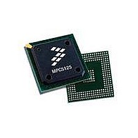
MPC5125YVN400 Freescale Semiconductor, MPC5125YVN400 Datasheet - Page 809

MPC5125YVN400
Manufacturer Part Number
MPC5125YVN400
Description
IC MCU 32BIT E300 324TEPBGA
Manufacturer
Freescale Semiconductor
Series
MPC51xxr
Datasheets
1.MPC5125YVN400.pdf
(92 pages)
2.MPC5125YVN400.pdf
(8 pages)
3.MPC5125YVN400.pdf
(2 pages)
4.MPC5125YVN400.pdf
(1064 pages)
Specifications of MPC5125YVN400
Core Processor
e300
Core Size
32-Bit
Speed
400MHz
Connectivity
CAN, EBI/EMI, Ethernet, I²C, USB OTG
Peripherals
DMA, WDT
Number Of I /o
64
Program Memory Type
ROMless
Ram Size
32K x 8
Voltage - Supply (vcc/vdd)
1.33 V ~ 1.47 V
Oscillator Type
External
Operating Temperature
-40°C ~ 125°C
Package / Case
324-PBGA
Processor Series
MPC51xx
Core
e300
Data Bus Width
32 bit
Development Tools By Supplier
TWR-MPC5125-KIT, TWR-SER, TWR-ELEV, TOWER
Maximum Clock Frequency
400 MHz
Operating Supply Voltage
1.4 V
Maximum Operating Temperature
+ 125 C
Mounting Style
SMD/SMT
Data Ram Size
32 KB
I/o Voltage
3.3 V
Interface Type
CAN, I2C
Minimum Operating Temperature
- 40 C
Program Memory Size
32 bit
Cpu Speed
400MHz
Embedded Interface Type
CAN, I2C, SPI, UART, USB
Digital Ic Case Style
TEPBGA
No. Of Pins
324
Rohs Compliant
Yes
Cpu Family
MPC5xx
Device Core Size
32b
Frequency (max)
400MHz
Total Internal Ram Size
32KB
Instruction Set Architecture
RISC
Operating Temp Range
-40C to 85C
Operating Temperature Classification
Industrial
Mounting
Surface Mount
Pin Count
324
Lead Free Status / RoHS Status
Lead free / RoHS Compliant
Eeprom Size
-
Program Memory Size
-
Data Converters
-
Lead Free Status / Rohs Status
Lead free / RoHS Compliant
Available stocks
Company
Part Number
Manufacturer
Quantity
Price
Company:
Part Number:
MPC5125YVN400
Manufacturer:
Freescale Semiconductor
Quantity:
135
Company:
Part Number:
MPC5125YVN400
Manufacturer:
LTC
Quantity:
29
Company:
Part Number:
MPC5125YVN400
Manufacturer:
Freescale Semiconductor
Quantity:
10 000
- MPC5125YVN400 PDF datasheet
- MPC5125YVN400 PDF datasheet #2
- MPC5125YVN400 PDF datasheet #3
- MPC5125YVN400 PDF datasheet #4
- Current page: 809 of 1064
- Download datasheet (6Mb)
write_reg(SDHC_STR_STP_CLK, 0x1);
write_reg(SDHC_STR_STP_CLK, 0x1);
write_reg(SDHC_STR_STP_CLK, 0x1);
write_reg(SDHC_STR_STP_CLK, 0x1);// 2. write 0x1 to SDHC_STR_STP_CLK 8 times;
write_reg(SDHC_STR_STP_CLK, 0x2); // 3. write 0x2 to SDHC_STR_STP_CLK to start clock;
while (!STATUS[8]); // 4. wait clock on
write_reg(SDHC_CLK_RATE, 0x3F);
write_reg(SDHC_READ_TO, 0x2DB4); // 6. set READ timeout register
send_cmd_wait_resp(CMD_GO_IDLE_STATE, 0x0,0x80, 0x40); //7. reset the card with CMD0
}
28.5.3.3
All cards are able to establish communication with the host using any operation voltage in the allowed
voltage range specified in the standard. However, the supported minimum and maximum voltages are
defined in the operation conditions register (OCR) and may not cover the whole range. Cards that store the
CID and CSD data in the preload memory can only communicate this information under data transfer V
conditions. If the host and card have non-compatible voltage ranges, the card cannot complete the
identification cycle nor send CSD data.
Therefore, a special command Send_Op_Cont (CMD1 for MMC), a SD_Send_Op_Cont (CMD41 for SD
Memory), and a IO_Send_Op_Cont (CMD5 for SD I/O) provide a mechanism to identify and reject cards
which do not match the voltage range desired by the host. The host accomplishes this by sending the
required voltage window as the operand of this command. Cards which cannot perform data transfer in the
specified range must disable themselves from further bus operations and go into the inactive state. By
omitting voltage range in the command, the host can query each card and determine the common voltage
range before sending out-of-range cards into inactive state. This query should be used if the host can select
a common voltage range or if a notification to the application of non-usable cards in the stack is desired.
The following steps show how to perform voltage validation when a card is inserted:
Freescale Semiconductor
voltage_validation(voltage_range_arguement)
{
send_cmd_wait_resp(IO_SEND_OP_COND, 0x0, 0x04, 0x40); // CMD5, send SDIO operation
voltage, command argument is zero
if(End Command Response true & No. of IO functions> 0)// it is SDIO and have IO function
{IORDY = 0;
while(!(IORDY in I/O ORC response)) {// set voltage range for each IO
send_cmd_wait_resp(IO_SEND_OP_COND, voltage_range_arguement, 0x04, 0x40);}
if(Memory Present flag true)
Card = combo; // that is, SDIO + SD Memory, need to set operation voltage to memory
portion as well
send_cmd_wait_resp(APP_CMD, 0x0, 0x01, 0x40);// CMD55, Application Command follows
send_cmd_wait_resp(SD_APP_OP_COND, voltage_range_argument, 0x01, 0x40);//ACMD41
else
Card = sdio;
// if No response to CMD5 IO_SEND_OP_COND or No. of IO Function is zero in response
else// the card should be SD or MMC
{send_cmd_wait_resp(APP_CMD, 0x0, 0x01, 0x40);// CMD55, Application Command follows
Voltage Validation
MPC5125 Microcontroller Reference Manual, Rev. 2
// 5. Set the lowest clock for initialization
Secure Digital Host Controller (SDHC)
28-37
DD
Related parts for MPC5125YVN400
Image
Part Number
Description
Manufacturer
Datasheet
Request
R
Part Number:
Description:
Mpc5125 Microcontroller Data Sheet
Manufacturer:
Freescale Semiconductor, Inc
Datasheet:

Part Number:
Description:
MPC5125 Microcontroller Data Sheet
Manufacturer:
FREESCALE [Freescale Semiconductor, Inc]
Datasheet:
Part Number:
Description:
Manufacturer:
Freescale Semiconductor, Inc
Datasheet:
Part Number:
Description:
Manufacturer:
Freescale Semiconductor, Inc
Datasheet:
Part Number:
Description:
Manufacturer:
Freescale Semiconductor, Inc
Datasheet:
Part Number:
Description:
Manufacturer:
Freescale Semiconductor, Inc
Datasheet:
Part Number:
Description:
Manufacturer:
Freescale Semiconductor, Inc
Datasheet:
Part Number:
Description:
Manufacturer:
Freescale Semiconductor, Inc
Datasheet:
Part Number:
Description:
Manufacturer:
Freescale Semiconductor, Inc
Datasheet:
Part Number:
Description:
Manufacturer:
Freescale Semiconductor, Inc
Datasheet:
Part Number:
Description:
Manufacturer:
Freescale Semiconductor, Inc
Datasheet:
Part Number:
Description:
Manufacturer:
Freescale Semiconductor, Inc
Datasheet:
Part Number:
Description:
Manufacturer:
Freescale Semiconductor, Inc
Datasheet:
Part Number:
Description:
Manufacturer:
Freescale Semiconductor, Inc
Datasheet:
Part Number:
Description:
Manufacturer:
Freescale Semiconductor, Inc
Datasheet:


