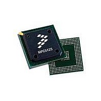
MPC5125YVN400 Freescale Semiconductor, MPC5125YVN400 Datasheet - Page 519

MPC5125YVN400
Manufacturer Part Number
MPC5125YVN400
Description
IC MCU 32BIT E300 324TEPBGA
Manufacturer
Freescale Semiconductor
Series
MPC51xxr
Datasheets
1.MPC5125YVN400.pdf
(92 pages)
2.MPC5125YVN400.pdf
(8 pages)
3.MPC5125YVN400.pdf
(2 pages)
4.MPC5125YVN400.pdf
(1064 pages)
Specifications of MPC5125YVN400
Core Processor
e300
Core Size
32-Bit
Speed
400MHz
Connectivity
CAN, EBI/EMI, Ethernet, I²C, USB OTG
Peripherals
DMA, WDT
Number Of I /o
64
Program Memory Type
ROMless
Ram Size
32K x 8
Voltage - Supply (vcc/vdd)
1.33 V ~ 1.47 V
Oscillator Type
External
Operating Temperature
-40°C ~ 125°C
Package / Case
324-PBGA
Processor Series
MPC51xx
Core
e300
Data Bus Width
32 bit
Development Tools By Supplier
TWR-MPC5125-KIT, TWR-SER, TWR-ELEV, TOWER
Maximum Clock Frequency
400 MHz
Operating Supply Voltage
1.4 V
Maximum Operating Temperature
+ 125 C
Mounting Style
SMD/SMT
Data Ram Size
32 KB
I/o Voltage
3.3 V
Interface Type
CAN, I2C
Minimum Operating Temperature
- 40 C
Program Memory Size
32 bit
Cpu Speed
400MHz
Embedded Interface Type
CAN, I2C, SPI, UART, USB
Digital Ic Case Style
TEPBGA
No. Of Pins
324
Rohs Compliant
Yes
Cpu Family
MPC5xx
Device Core Size
32b
Frequency (max)
400MHz
Total Internal Ram Size
32KB
Instruction Set Architecture
RISC
Operating Temp Range
-40C to 85C
Operating Temperature Classification
Industrial
Mounting
Surface Mount
Pin Count
324
Lead Free Status / RoHS Status
Lead free / RoHS Compliant
Eeprom Size
-
Program Memory Size
-
Data Converters
-
Lead Free Status / Rohs Status
Lead free / RoHS Compliant
Available stocks
Company
Part Number
Manufacturer
Quantity
Price
Company:
Part Number:
MPC5125YVN400
Manufacturer:
Freescale Semiconductor
Quantity:
135
Company:
Part Number:
MPC5125YVN400
Manufacturer:
LTC
Quantity:
29
Company:
Part Number:
MPC5125YVN400
Manufacturer:
Freescale Semiconductor
Quantity:
10 000
- MPC5125YVN400 PDF datasheet
- MPC5125YVN400 PDF datasheet #2
- MPC5125YVN400 PDF datasheet #3
- MPC5125YVN400 PDF datasheet #4
- Current page: 519 of 1064
- Download datasheet (6Mb)
Chapter 20
I/O Control
20.1
20.1.1
The I/O control block controls the functional muxing and configuration of the pads. Configurable
parameters include slew rate, Schmitt trigger input and pull-down/up, and a global Output Buffer Enable
(OBE).
20.1.2
20.2
20.2.1
Freescale Semiconductor
IOCONTROL_BASE
(0xFF40_A000)
0x002–0x003
•
•
•
•
•
Offset from
0x000
0x001
0x004
0x005
0x006
0x007
0x008
Functional pin muxing control
Pad slew rate control
Pad Schmitt trigger control
Pad pull-down/pull-up control
Global OBE control
Introduction
Memory Map and Register Definition
Overview
Features
Memory Map
1
IO_CTL_MEM—MEM pad control register
IO_CTL_GBOBE—Global Output Enable Control Register
Reserved
IO_CTL_LPC_CLK—LPC_CLK pad control register (STD_PU)
IO_CTL_LPC_OE_B— PC_OE_B pad control register (STD_PU)
IO_CTL_LPC_RWB—LPC_RWB pad control register (STD_PU)
IO_CTL_LPC_CS0_B—LPC_CS0_B pad control register (STD_PU)
IO_CTL_LPC_ACK_B—LPC_ACK_B pad control register (STD_PU)
MPC5125 Microcontroller Reference Manual, Rev. 2
Table 20-1. I/O Control Memory Map
Register
2
Access
R/W
R/W
R/W
R/W
R/W
R/W
R/W
Reset
Value
0x1B
0x1B
0x00
0x00
0x03
0x03
0x03
Section/Page
20.2.2.3.1/20-8
20.2.2.3.1/20-8
20.2.2.3.1/20-8
20.2.2.3.1/20-8
20.2.2.3.1/20-8
20.2.2.1/20-6
20.2.2.2/20-7
20-1
Related parts for MPC5125YVN400
Image
Part Number
Description
Manufacturer
Datasheet
Request
R
Part Number:
Description:
Mpc5125 Microcontroller Data Sheet
Manufacturer:
Freescale Semiconductor, Inc
Datasheet:

Part Number:
Description:
MPC5125 Microcontroller Data Sheet
Manufacturer:
FREESCALE [Freescale Semiconductor, Inc]
Datasheet:
Part Number:
Description:
Manufacturer:
Freescale Semiconductor, Inc
Datasheet:
Part Number:
Description:
Manufacturer:
Freescale Semiconductor, Inc
Datasheet:
Part Number:
Description:
Manufacturer:
Freescale Semiconductor, Inc
Datasheet:
Part Number:
Description:
Manufacturer:
Freescale Semiconductor, Inc
Datasheet:
Part Number:
Description:
Manufacturer:
Freescale Semiconductor, Inc
Datasheet:
Part Number:
Description:
Manufacturer:
Freescale Semiconductor, Inc
Datasheet:
Part Number:
Description:
Manufacturer:
Freescale Semiconductor, Inc
Datasheet:
Part Number:
Description:
Manufacturer:
Freescale Semiconductor, Inc
Datasheet:
Part Number:
Description:
Manufacturer:
Freescale Semiconductor, Inc
Datasheet:
Part Number:
Description:
Manufacturer:
Freescale Semiconductor, Inc
Datasheet:
Part Number:
Description:
Manufacturer:
Freescale Semiconductor, Inc
Datasheet:
Part Number:
Description:
Manufacturer:
Freescale Semiconductor, Inc
Datasheet:
Part Number:
Description:
Manufacturer:
Freescale Semiconductor, Inc
Datasheet:


