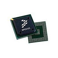
MPC5125YVN400 Freescale Semiconductor, MPC5125YVN400 Datasheet - Page 562

MPC5125YVN400
Manufacturer Part Number
MPC5125YVN400
Description
IC MCU 32BIT E300 324TEPBGA
Manufacturer
Freescale Semiconductor
Series
MPC51xxr
Datasheets
1.MPC5125YVN400.pdf
(92 pages)
2.MPC5125YVN400.pdf
(8 pages)
3.MPC5125YVN400.pdf
(2 pages)
4.MPC5125YVN400.pdf
(1064 pages)
Specifications of MPC5125YVN400
Core Processor
e300
Core Size
32-Bit
Speed
400MHz
Connectivity
CAN, EBI/EMI, Ethernet, I²C, USB OTG
Peripherals
DMA, WDT
Number Of I /o
64
Program Memory Type
ROMless
Ram Size
32K x 8
Voltage - Supply (vcc/vdd)
1.33 V ~ 1.47 V
Oscillator Type
External
Operating Temperature
-40°C ~ 125°C
Package / Case
324-PBGA
Processor Series
MPC51xx
Core
e300
Data Bus Width
32 bit
Development Tools By Supplier
TWR-MPC5125-KIT, TWR-SER, TWR-ELEV, TOWER
Maximum Clock Frequency
400 MHz
Operating Supply Voltage
1.4 V
Maximum Operating Temperature
+ 125 C
Mounting Style
SMD/SMT
Data Ram Size
32 KB
I/o Voltage
3.3 V
Interface Type
CAN, I2C
Minimum Operating Temperature
- 40 C
Program Memory Size
32 bit
Cpu Speed
400MHz
Embedded Interface Type
CAN, I2C, SPI, UART, USB
Digital Ic Case Style
TEPBGA
No. Of Pins
324
Rohs Compliant
Yes
Cpu Family
MPC5xx
Device Core Size
32b
Frequency (max)
400MHz
Total Internal Ram Size
32KB
Instruction Set Architecture
RISC
Operating Temp Range
-40C to 85C
Operating Temperature Classification
Industrial
Mounting
Surface Mount
Pin Count
324
Lead Free Status / RoHS Status
Lead free / RoHS Compliant
Eeprom Size
-
Program Memory Size
-
Data Converters
-
Lead Free Status / Rohs Status
Lead free / RoHS Compliant
Available stocks
Company
Part Number
Manufacturer
Quantity
Price
Company:
Part Number:
MPC5125YVN400
Manufacturer:
Freescale Semiconductor
Quantity:
135
Company:
Part Number:
MPC5125YVN400
Manufacturer:
LTC
Quantity:
29
Company:
Part Number:
MPC5125YVN400
Manufacturer:
Freescale Semiconductor
Quantity:
10 000
- MPC5125YVN400 PDF datasheet
- MPC5125YVN400 PDF datasheet #2
- MPC5125YVN400 PDF datasheet #3
- MPC5125YVN400 PDF datasheet #4
- Current page: 562 of 1064
- Download datasheet (6Mb)
LocalPlus Bus Controller (LPC)
21.3
There are two primary modes of operation:
Within each mode, there is considerable flexibility to control the operation.
Each CS can be programmed to a different mode of operation (muxed, non-muxed, number of wait states,
byte swapping, etc.).
In muxed mode, the same 32-bit local bus presents an address in an address tenure and data in a data tenure,
in a muxed fashion (similar to PCI protocol).
Muxed mode provides an ALE during the address phase to capture the address. This mode requires
external logic to latch the address during the address tenure. The level of the ALE can be programmed by
the ALE bit.
An ACK input is provided and can be asserted to shorten (but not extend) wait states.
The LPC on MPC5125 provides an output enable signal, OE, to achieve a complete glueless interface for
most devices. OE is asserted one clock after the CS assertion if a read transaction occurs.
Muxed and non-muxed modes support a variety of device configurations and are configurable on a per CS
basis. The read and write burst functionality is available in both modes. In non-muxed mode, an
asynchronous burst (page mode burst) is also possible.
21.3.1
In non-muxed mode, the 32-bit address/data bus is divided into address and/or data lines.
21-22
ALARM_W
•
•
Field
Muxed
Non-muxed
Functional Description
Non-Muxed Mode
Alarm Watermark. Write these bits to set the low (write)/high (read) level watermark, which is the point where
FIFO asserts a request for the DMA controller data to fill (write)/empty (read). The value is in bytes.
For example, During a SCLPC write operation (R/W bit of SCLPC Control (LPC_SCLPC_C) Register) and an
alarm watermark setting of 128, an alarm condition occurs when FIFO contains 128 bytes or less.
After asserted, an alarm does not negate until a high (write)/ low (read) level mark is reached, as specified by
the LPC RX/TX FIFO Control (LPC_SCLPC_FIFOC) Register granularity bits.
Data Size
16
16
8
Table 21-23. LPC_SCLPC_FIFOA field descriptions
MPC5125 Microcontroller Reference Manual, Rev. 2
Bus Width
Address
Table 21-24. Non-Muxed Mode Options
32
26
26
Pins Used
40
42
42
Description
Memory Size
128 MB
64 MB
4 GB
Short addressing
Byte addressing
Comments
Freescale Semiconductor
Related parts for MPC5125YVN400
Image
Part Number
Description
Manufacturer
Datasheet
Request
R
Part Number:
Description:
Mpc5125 Microcontroller Data Sheet
Manufacturer:
Freescale Semiconductor, Inc
Datasheet:

Part Number:
Description:
MPC5125 Microcontroller Data Sheet
Manufacturer:
FREESCALE [Freescale Semiconductor, Inc]
Datasheet:
Part Number:
Description:
Manufacturer:
Freescale Semiconductor, Inc
Datasheet:
Part Number:
Description:
Manufacturer:
Freescale Semiconductor, Inc
Datasheet:
Part Number:
Description:
Manufacturer:
Freescale Semiconductor, Inc
Datasheet:
Part Number:
Description:
Manufacturer:
Freescale Semiconductor, Inc
Datasheet:
Part Number:
Description:
Manufacturer:
Freescale Semiconductor, Inc
Datasheet:
Part Number:
Description:
Manufacturer:
Freescale Semiconductor, Inc
Datasheet:
Part Number:
Description:
Manufacturer:
Freescale Semiconductor, Inc
Datasheet:
Part Number:
Description:
Manufacturer:
Freescale Semiconductor, Inc
Datasheet:
Part Number:
Description:
Manufacturer:
Freescale Semiconductor, Inc
Datasheet:
Part Number:
Description:
Manufacturer:
Freescale Semiconductor, Inc
Datasheet:
Part Number:
Description:
Manufacturer:
Freescale Semiconductor, Inc
Datasheet:
Part Number:
Description:
Manufacturer:
Freescale Semiconductor, Inc
Datasheet:
Part Number:
Description:
Manufacturer:
Freescale Semiconductor, Inc
Datasheet:


