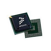
MPC5125YVN400 Freescale Semiconductor, MPC5125YVN400 Datasheet - Page 328

MPC5125YVN400
Manufacturer Part Number
MPC5125YVN400
Description
IC MCU 32BIT E300 324TEPBGA
Manufacturer
Freescale Semiconductor
Series
MPC51xxr
Datasheets
1.MPC5125YVN400.pdf
(92 pages)
2.MPC5125YVN400.pdf
(8 pages)
3.MPC5125YVN400.pdf
(2 pages)
4.MPC5125YVN400.pdf
(1064 pages)
Specifications of MPC5125YVN400
Core Processor
e300
Core Size
32-Bit
Speed
400MHz
Connectivity
CAN, EBI/EMI, Ethernet, I²C, USB OTG
Peripherals
DMA, WDT
Number Of I /o
64
Program Memory Type
ROMless
Ram Size
32K x 8
Voltage - Supply (vcc/vdd)
1.33 V ~ 1.47 V
Oscillator Type
External
Operating Temperature
-40°C ~ 125°C
Package / Case
324-PBGA
Processor Series
MPC51xx
Core
e300
Data Bus Width
32 bit
Development Tools By Supplier
TWR-MPC5125-KIT, TWR-SER, TWR-ELEV, TOWER
Maximum Clock Frequency
400 MHz
Operating Supply Voltage
1.4 V
Maximum Operating Temperature
+ 125 C
Mounting Style
SMD/SMT
Data Ram Size
32 KB
I/o Voltage
3.3 V
Interface Type
CAN, I2C
Minimum Operating Temperature
- 40 C
Program Memory Size
32 bit
Cpu Speed
400MHz
Embedded Interface Type
CAN, I2C, SPI, UART, USB
Digital Ic Case Style
TEPBGA
No. Of Pins
324
Rohs Compliant
Yes
Cpu Family
MPC5xx
Device Core Size
32b
Frequency (max)
400MHz
Total Internal Ram Size
32KB
Instruction Set Architecture
RISC
Operating Temp Range
-40C to 85C
Operating Temperature Classification
Industrial
Mounting
Surface Mount
Pin Count
324
Lead Free Status / RoHS Status
Lead free / RoHS Compliant
Eeprom Size
-
Program Memory Size
-
Data Converters
-
Lead Free Status / Rohs Status
Lead free / RoHS Compliant
Available stocks
Company
Part Number
Manufacturer
Quantity
Price
Company:
Part Number:
MPC5125YVN400
Manufacturer:
Freescale Semiconductor
Quantity:
135
Company:
Part Number:
MPC5125YVN400
Manufacturer:
LTC
Quantity:
29
Company:
Part Number:
MPC5125YVN400
Manufacturer:
Freescale Semiconductor
Quantity:
10 000
- MPC5125YVN400 PDF datasheet
- MPC5125YVN400 PDF datasheet #2
- MPC5125YVN400 PDF datasheet #3
- MPC5125YVN400 PDF datasheet #4
- Current page: 328 of 1064
- Download datasheet (6Mb)
DRAM Controller
During SDR mode, DQS is driven by the device all the time. DQS is driven out by the controller
synchronous with DRAM_CLK the specified CAS delay after the read command was issued. Read data is
input relative to the DQS, exactly the same way as it happens in DDR mode. This means, the strobe point
is 1/4 clock after the edges of the DQS.
It is possible to shift the sample point to right after the clock edges of DQS by writing 0x2020_2020 to the
DQS Config Offset Time register.
11.4
The DRAM controller is a multi-port DRAM controller. It listens to incoming requests on multiple buses
and decides on each rising clock edge what command needs to be sent to the DRAM.
A block diagram is given in
following sections.
11.4.1
11.4.1.1
11-20
DRAM_TIME_WTR1_OTHER[3:0] For description, refer to
DRAM_COMMAND
DRAM_TIME_CCD_OTHER[3:0] For description, refer to
DRAM_ADDRESS
•
DRAM_CS_SELECT[3:0]
DRAM_DQS
DRAM_CLK
32-bit DRAM systems need to be connected to all DQ, DM, DQS lines.
DRAM_DQ
CONFIG_CAS3
CONFIG_SDR
CONFIG_A15
Functional Description
Interfacing with the DRAM
Field
Connecting the DRAM
Bank A
READ
Figure
Table 11-17. EXTRA_ATTRIB field descriptions
MPC5125 Microcontroller Reference Manual, Rev. 2
0 DDR mode.
1 SDR mode.
0 SDR timing with CAS latency 2.
1 SDR timing with CAS latency 3.
0 A15 pin acts as A15.
1 A15 pin acts as Chip Select 1.
For description, refer to
Figure 11-19. SDR read timing diagram
11-1. The major blocks of the DRAM controller are described in the
Table
Table
Table
11-9.
11-9.
11-7.
D1
Description
D2
D3
Freescale Semiconductor
D4
Related parts for MPC5125YVN400
Image
Part Number
Description
Manufacturer
Datasheet
Request
R
Part Number:
Description:
Mpc5125 Microcontroller Data Sheet
Manufacturer:
Freescale Semiconductor, Inc
Datasheet:

Part Number:
Description:
MPC5125 Microcontroller Data Sheet
Manufacturer:
FREESCALE [Freescale Semiconductor, Inc]
Datasheet:
Part Number:
Description:
Manufacturer:
Freescale Semiconductor, Inc
Datasheet:
Part Number:
Description:
Manufacturer:
Freescale Semiconductor, Inc
Datasheet:
Part Number:
Description:
Manufacturer:
Freescale Semiconductor, Inc
Datasheet:
Part Number:
Description:
Manufacturer:
Freescale Semiconductor, Inc
Datasheet:
Part Number:
Description:
Manufacturer:
Freescale Semiconductor, Inc
Datasheet:
Part Number:
Description:
Manufacturer:
Freescale Semiconductor, Inc
Datasheet:
Part Number:
Description:
Manufacturer:
Freescale Semiconductor, Inc
Datasheet:
Part Number:
Description:
Manufacturer:
Freescale Semiconductor, Inc
Datasheet:
Part Number:
Description:
Manufacturer:
Freescale Semiconductor, Inc
Datasheet:
Part Number:
Description:
Manufacturer:
Freescale Semiconductor, Inc
Datasheet:
Part Number:
Description:
Manufacturer:
Freescale Semiconductor, Inc
Datasheet:
Part Number:
Description:
Manufacturer:
Freescale Semiconductor, Inc
Datasheet:
Part Number:
Description:
Manufacturer:
Freescale Semiconductor, Inc
Datasheet:


