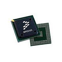
MPC5125YVN400 Freescale Semiconductor, MPC5125YVN400 Datasheet - Page 644

MPC5125YVN400
Manufacturer Part Number
MPC5125YVN400
Description
IC MCU 32BIT E300 324TEPBGA
Manufacturer
Freescale Semiconductor
Series
MPC51xxr
Datasheets
1.MPC5125YVN400.pdf
(92 pages)
2.MPC5125YVN400.pdf
(8 pages)
3.MPC5125YVN400.pdf
(2 pages)
4.MPC5125YVN400.pdf
(1064 pages)
Specifications of MPC5125YVN400
Core Processor
e300
Core Size
32-Bit
Speed
400MHz
Connectivity
CAN, EBI/EMI, Ethernet, I²C, USB OTG
Peripherals
DMA, WDT
Number Of I /o
64
Program Memory Type
ROMless
Ram Size
32K x 8
Voltage - Supply (vcc/vdd)
1.33 V ~ 1.47 V
Oscillator Type
External
Operating Temperature
-40°C ~ 125°C
Package / Case
324-PBGA
Processor Series
MPC51xx
Core
e300
Data Bus Width
32 bit
Development Tools By Supplier
TWR-MPC5125-KIT, TWR-SER, TWR-ELEV, TOWER
Maximum Clock Frequency
400 MHz
Operating Supply Voltage
1.4 V
Maximum Operating Temperature
+ 125 C
Mounting Style
SMD/SMT
Data Ram Size
32 KB
I/o Voltage
3.3 V
Interface Type
CAN, I2C
Minimum Operating Temperature
- 40 C
Program Memory Size
32 bit
Cpu Speed
400MHz
Embedded Interface Type
CAN, I2C, SPI, UART, USB
Digital Ic Case Style
TEPBGA
No. Of Pins
324
Rohs Compliant
Yes
Cpu Family
MPC5xx
Device Core Size
32b
Frequency (max)
400MHz
Total Internal Ram Size
32KB
Instruction Set Architecture
RISC
Operating Temp Range
-40C to 85C
Operating Temperature Classification
Industrial
Mounting
Surface Mount
Pin Count
324
Lead Free Status / RoHS Status
Lead free / RoHS Compliant
Eeprom Size
-
Program Memory Size
-
Data Converters
-
Lead Free Status / Rohs Status
Lead free / RoHS Compliant
Available stocks
Company
Part Number
Manufacturer
Quantity
Price
Company:
Part Number:
MPC5125YVN400
Manufacturer:
Freescale Semiconductor
Quantity:
135
Company:
Part Number:
MPC5125YVN400
Manufacturer:
LTC
Quantity:
29
Company:
Part Number:
MPC5125YVN400
Manufacturer:
Freescale Semiconductor
Quantity:
10 000
- MPC5125YVN400 PDF datasheet
- MPC5125YVN400 PDF datasheet #2
- MPC5125YVN400 PDF datasheet #3
- MPC5125YVN400 PDF datasheet #4
- Current page: 644 of 1064
- Download datasheet (6Mb)
NAND Flash Controller (NFC)
23.7.11 Cache Swap register (CACHE_SWAP)
Note: When DMA transfers data to/from the NFC cache(NFC SRAM buffer), or when CPU reads or writes data to/from the NFC
The feature is added to the flash controller to allow to have the bad block marker in the first position of the spare area of a page.
Because of the way the flash controller interleaves data and ECC bytes on flash devices with page sizes larger than 2 KB, the
position of the bad block marker is shifted, and will not appear in the first position of the spare area of the page any more. The
cache swap feature allows consistent swapping of the “actual” bad block line with the “expected” bad block line, and causes the
operating system to get the bad block marker in the position where it is expected.
23-14
Address: Base + 0x3F28
DMA2_OFFSET[11:1]
CACHE_SWAP_ADDR1[13:3]
CACHE_SWAP_ADDR2[13:3]
Reset
Reset
DMA1_CNT[11:0]
DMA2_CNT[6:0]
cache via the IPS bus, all accesses that should go to CACHE_SWAP_ADDR1, are directed to CACHE_SWAP_ADDR2,
and all accesses that should go to CACHE_SWAP_ADDR2 are directed to CACHE_SWAP_ADDR1.
DMA1_ACT
DMA2_ACT
W
W
R
R
Field
16
0
0
0
0
0
Field
17
0
0
0
0
1
Byte count to be transferred by DMA for DMA channel 1.
Byte count to be transferred by DMA for DMA channel 2.
Byte offset for DMA channel 2. DMA channel 2 transfer start s at this offset count. DMA2_OFFSET
must be 256 bytes aligned, so DMA2_OFFSET[7:1] should be always 0.
DMA Channel 1 Activity
0 DMA channel 1 is inactive.
1 DMA channel 1 is active, and will be used for transfer to memory when triggered.
DMA Channel 2 Activity
0 DMA channel 2 is inactive.
1 DMA channel 2 is active, and is used for transfer to memory when triggered.
18
0
0
0
0
2
Figure 23-13. Cache Swap register (CACHE_SWAP)
19
0
0
0
0
3
MPC5125 Microcontroller Reference Manual, Rev. 2
Table 23-14. CACHE_SWAP field descriptions
Table 23-13. DMA_CONFIG field descriptions
Lower swap address.
Upper swap address.
20
4
1
1
21
1
1
5
22
1
1
6
23
1
1
7
CACHE_SWAP_ADDR2[13:3]
CACHE_SWAP_ADDR1[13:3]
Description
24
8
1
1
Description
25
9
1
1
Table 23-21
10
26
1
1
11
27
1
1
gives some examples of usage.
12
28
1
1
Freescale Semiconductor
Access: User read/write
13
29
1
1
14
30
1
1
15
31
0
0
0
0
Related parts for MPC5125YVN400
Image
Part Number
Description
Manufacturer
Datasheet
Request
R
Part Number:
Description:
Mpc5125 Microcontroller Data Sheet
Manufacturer:
Freescale Semiconductor, Inc
Datasheet:

Part Number:
Description:
MPC5125 Microcontroller Data Sheet
Manufacturer:
FREESCALE [Freescale Semiconductor, Inc]
Datasheet:
Part Number:
Description:
Manufacturer:
Freescale Semiconductor, Inc
Datasheet:
Part Number:
Description:
Manufacturer:
Freescale Semiconductor, Inc
Datasheet:
Part Number:
Description:
Manufacturer:
Freescale Semiconductor, Inc
Datasheet:
Part Number:
Description:
Manufacturer:
Freescale Semiconductor, Inc
Datasheet:
Part Number:
Description:
Manufacturer:
Freescale Semiconductor, Inc
Datasheet:
Part Number:
Description:
Manufacturer:
Freescale Semiconductor, Inc
Datasheet:
Part Number:
Description:
Manufacturer:
Freescale Semiconductor, Inc
Datasheet:
Part Number:
Description:
Manufacturer:
Freescale Semiconductor, Inc
Datasheet:
Part Number:
Description:
Manufacturer:
Freescale Semiconductor, Inc
Datasheet:
Part Number:
Description:
Manufacturer:
Freescale Semiconductor, Inc
Datasheet:
Part Number:
Description:
Manufacturer:
Freescale Semiconductor, Inc
Datasheet:
Part Number:
Description:
Manufacturer:
Freescale Semiconductor, Inc
Datasheet:
Part Number:
Description:
Manufacturer:
Freescale Semiconductor, Inc
Datasheet:


