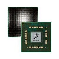
MPC8536DS Freescale Semiconductor, MPC8536DS Datasheet - Page 996

MPC8536DS
Manufacturer Part Number
MPC8536DS
Description
BOARD DEV SYSTEM MPC8536E
Manufacturer
Freescale Semiconductor
Series
PowerQUICC III™r
Type
MPUr
Datasheets
1.MPC8536EBVTAVLA.pdf
(127 pages)
2.MPC8536EBVTAVLA.pdf
(1706 pages)
3.MPC8536DS.pdf
(2 pages)
4.MPC8536DS.pdf
(126 pages)
Specifications of MPC8536DS
Contents
Board, Software and Documentation
Processor Series
MPC85xx
Core
e500
Data Bus Width
32 bit
Maximum Clock Frequency
667 MHz
Operating Supply Voltage
- 0.3 V to + 1.21 V
Maximum Operating Temperature
+ 105 C
Data Ram Size
32 KB
Interface Type
SPI, USB
Program Memory Type
DDR2, DDR3, SDRAM
Core Size
32 Bit
Program Memory Size
544KB
Cpu Speed
1.5GHz
Digital Ic Case Style
BGA
No. Of Pins
783
Supply Voltage Range
0.95V To 1.05V
Rohs Compliant
Yes
For Use With/related Products
MPC8536
Lead Free Status / RoHS Status
Lead free / RoHS Compliant
- MPC8536EBVTAVLA PDF datasheet
- MPC8536EBVTAVLA PDF datasheet #2
- MPC8536DS PDF datasheet #3
- MPC8536DS PDF datasheet #4
- Current page: 996 of 1706
- Download datasheet (15Mb)
DMA Controller
15-10
14–15
16–17
Bits
18
19
20
21
22
23
24
25
EOLNIE End-of-links interrupt enable
EOLSIE End-of-lists interrupt enable
DAHTS Destination address hold transfer size. Indicates the transfer size used for each transaction while
SAHTS Source address hold transfer size. Indicates the transfer size used for each transaction while MR n [SAHE]
EOSIE
Name
DAHE
SAHE
SRW
EIE
—
MR n [DAHE] is set. The byte count register must be in multiples of the size and the destination address
register must be aligned based on the size. The transfer size assigned to MR n [DAHTS] must be equal to or
smaller than that assigned to MR n [BWC] to avoid undefined behavior.
00 1 byte
01 2 bytes
10 4 bytes
11 8 bytes
is set. The byte count register must be in multiples of the size and the source address register must be
aligned based on the size. The transfer size assigned to MR n [SAHTS] must be equal to or smaller than that
assigned to MR n [BWC] to avoid undefined behavior.
00 1 byte
01 2 bytes
10 4 bytes
11 8 bytes
0 Disable destination address hold
1 Enable the DMA controller to hold the destination address of a transfer to the size specified by
0 Disable source address hold
1 Enable the DMA controller to hold the source address of a transfer to the size specified by MR n [SAHTS].
Reserved
0 Normal operation
1 Enable a write to the source address register to simultaneously set MR n [CS], starting a DMA transfer,
0 Do not generate an interrupt at the completion of a data transfer. CLNDAR n [EOSIE] overrides this bit on
1 Generate an interrupt at the completion of a data transfer (That is, SR n [EOSI] is set). This bit overrides
0 Do not generate an interrupt at the completion of a list of DMA transfers.
1 Generate an interrupt at the completion of a list of DMA transfers (That is, NLNDAR n [EOLND] is set).
0 Do not generate an interrupt at the completion of all DMA transfers.
1 Generate an interrupt at the completion of all DMA transfers (That is, NLNDAR n [EOLND] and
0 Do not generate an interrupt if a programming or transfer error is detected.
1 Generate an interrupt if a programming or transfer error is detected.
Destination address hold enable
Source address hold enable
Single register write (Direct mode only; reserved for chaining mode.)
End-of-segments interrupt enable
Error interrupt enable
MR n [DAHTS]. Hardware only supports aligned transfers for this feature.
Hardware only supports aligned transfers for this feature.
when MR n [CDSM/SWSM] is also set. Setting this bit and clearing CDSM/SWSM causes a write to the
destination address register to simultaneously set MR n [CS], starting a DMA transfer.
a link descriptor basis.
the CLNDAR n [EOSIE].
NLSDAR n [EOLSD] are set).
MPC8536E PowerQUICC III Integrated Processor Reference Manual, Rev. 1
Table 15-5. MR n Field Descriptions (continued)
Description
Freescale Semiconductor
Related parts for MPC8536DS
Image
Part Number
Description
Manufacturer
Datasheet
Request
R
Part Number:
Description:
Manufacturer:
Freescale Semiconductor, Inc
Datasheet:
Part Number:
Description:
Manufacturer:
Freescale Semiconductor, Inc
Datasheet:
Part Number:
Description:
Manufacturer:
Freescale Semiconductor, Inc
Datasheet:
Part Number:
Description:
Manufacturer:
Freescale Semiconductor, Inc
Datasheet:
Part Number:
Description:
Manufacturer:
Freescale Semiconductor, Inc
Datasheet:
Part Number:
Description:
Manufacturer:
Freescale Semiconductor, Inc
Datasheet:
Part Number:
Description:
Manufacturer:
Freescale Semiconductor, Inc
Datasheet:
Part Number:
Description:
Manufacturer:
Freescale Semiconductor, Inc
Datasheet:
Part Number:
Description:
Manufacturer:
Freescale Semiconductor, Inc
Datasheet:
Part Number:
Description:
Manufacturer:
Freescale Semiconductor, Inc
Datasheet:
Part Number:
Description:
Manufacturer:
Freescale Semiconductor, Inc
Datasheet:
Part Number:
Description:
Manufacturer:
Freescale Semiconductor, Inc
Datasheet:
Part Number:
Description:
Manufacturer:
Freescale Semiconductor, Inc
Datasheet:
Part Number:
Description:
Manufacturer:
Freescale Semiconductor, Inc
Datasheet:
Part Number:
Description:
Manufacturer:
Freescale Semiconductor, Inc
Datasheet:


