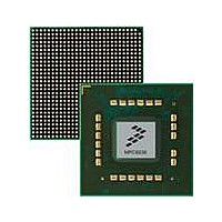
MPC8536DS Freescale Semiconductor, MPC8536DS Datasheet - Page 358

MPC8536DS
Manufacturer Part Number
MPC8536DS
Description
BOARD DEV SYSTEM MPC8536E
Manufacturer
Freescale Semiconductor
Series
PowerQUICC III™r
Type
MPUr
Datasheets
1.MPC8536EBVTAVLA.pdf
(127 pages)
2.MPC8536EBVTAVLA.pdf
(1706 pages)
3.MPC8536DS.pdf
(2 pages)
4.MPC8536DS.pdf
(126 pages)
Specifications of MPC8536DS
Contents
Board, Software and Documentation
Processor Series
MPC85xx
Core
e500
Data Bus Width
32 bit
Maximum Clock Frequency
667 MHz
Operating Supply Voltage
- 0.3 V to + 1.21 V
Maximum Operating Temperature
+ 105 C
Data Ram Size
32 KB
Interface Type
SPI, USB
Program Memory Type
DDR2, DDR3, SDRAM
Core Size
32 Bit
Program Memory Size
544KB
Cpu Speed
1.5GHz
Digital Ic Case Style
BGA
No. Of Pins
783
Supply Voltage Range
0.95V To 1.05V
Rohs Compliant
Yes
For Use With/related Products
MPC8536
Lead Free Status / RoHS Status
Lead free / RoHS Compliant
- MPC8536EBVTAVLA PDF datasheet
- MPC8536EBVTAVLA PDF datasheet #2
- MPC8536DS PDF datasheet #3
- MPC8536DS PDF datasheet #4
- Current page: 358 of 1706
- Download datasheet (15Mb)
DDR Memory Controller
Page mode can dramatically reduce access latencies for page hits. Depending on the memory system
design and timing parameters, using page mode can save two to three clock cycles for subsequent burst
accesses that hit in an active page. Also, better performance can be obtained using more banks, especially
in systems which use many different channels. Page mode is disabled by clearing
DDR_SDRAM_INTERVAL[BSTOPRE] or setting CSn_CONFIG[AP_nEN].
8.5.11
The DDR memory controller supports error checking and correcting (ECC) for the data path between the
core master and system memory. The memory detects all double-bit errors, detects all multi-bit errors
within a nibble, and corrects all single-bit errors. Other errors may be detected, but are not guaranteed to
be corrected or detected. Multiple-bit errors are always reported when error reporting is enabled. When a
single-bit error occurs, the single-bit error counter register is incremented, and its value compared to the
single-bit error trigger register. An error is reported when these values are equal. The single-bit error
registers can be programmed such that minor memory faults are corrected and ignored, but a catastrophic
memory failure generates an interrupt.
For writes that are smaller than 64 bits, the DDR memory controller performs a double-word read from
system memory of the address for the write (checking for errors), and merges the write data with the data
read from memory. Then, a new ECC code is generated for the merged double word. The data and ECC
code is then written to memory. If a multi-bit error is detected on the read, the transaction completes the
read-modify-write to keep the DDR memory controller from hanging. However, the corrupt data is masked
on the write, so the original contents in SDRAM remain unchanged.
The syndrome encodings for the ECC code are shown in
In 32-bit mode,
the ECC bits for the first 32 data bits of any 64-bit granule of data. This always applies to the odd data
beats on the DDR data bus. The second half of the table, consisting of rows 32–63, is used to calculate the
ECC bits for the second 32 bits of any 64-bit granule of data. This always applies to the even data beats
on the DDR data bus.
8-84
•
There is a logical bank row collision with another transaction that must be issued.
Data
Bit
0
1
2
3
4
5
6
7
Error Checking and Correcting (ECC)
Table 8-65
0
•
•
•
•
•
•
•
•
MPC8536E PowerQUICC III Integrated Processor Reference Manual, Rev. 1
1
•
•
2
•
•
Syndrome Bit
is split into 2 halves. The first half, consisting of rows 0–31, is used to calculate
Table 8-65. DDR SDRAM ECC Syndrome Encoding
3
•
•
4
•
•
5
•
•
•
•
6
7
•
•
•
•
Table 8-65
Data
Bit
32
33
34
35
36
37
38
39
0
•
•
and
1
•
•
Table
2
•
•
•
•
•
•
•
•
Syndrome Bit
8-66.
3
•
•
4
•
•
•
•
•
•
Freescale Semiconductor
5
•
•
•
•
6
7
•
•
•
•
Related parts for MPC8536DS
Image
Part Number
Description
Manufacturer
Datasheet
Request
R
Part Number:
Description:
Manufacturer:
Freescale Semiconductor, Inc
Datasheet:
Part Number:
Description:
Manufacturer:
Freescale Semiconductor, Inc
Datasheet:
Part Number:
Description:
Manufacturer:
Freescale Semiconductor, Inc
Datasheet:
Part Number:
Description:
Manufacturer:
Freescale Semiconductor, Inc
Datasheet:
Part Number:
Description:
Manufacturer:
Freescale Semiconductor, Inc
Datasheet:
Part Number:
Description:
Manufacturer:
Freescale Semiconductor, Inc
Datasheet:
Part Number:
Description:
Manufacturer:
Freescale Semiconductor, Inc
Datasheet:
Part Number:
Description:
Manufacturer:
Freescale Semiconductor, Inc
Datasheet:
Part Number:
Description:
Manufacturer:
Freescale Semiconductor, Inc
Datasheet:
Part Number:
Description:
Manufacturer:
Freescale Semiconductor, Inc
Datasheet:
Part Number:
Description:
Manufacturer:
Freescale Semiconductor, Inc
Datasheet:
Part Number:
Description:
Manufacturer:
Freescale Semiconductor, Inc
Datasheet:
Part Number:
Description:
Manufacturer:
Freescale Semiconductor, Inc
Datasheet:
Part Number:
Description:
Manufacturer:
Freescale Semiconductor, Inc
Datasheet:
Part Number:
Description:
Manufacturer:
Freescale Semiconductor, Inc
Datasheet:


