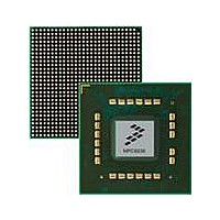
MPC8536DS Freescale Semiconductor, MPC8536DS Datasheet - Page 143

MPC8536DS
Manufacturer Part Number
MPC8536DS
Description
BOARD DEV SYSTEM MPC8536E
Manufacturer
Freescale Semiconductor
Series
PowerQUICC III™r
Type
MPUr
Datasheets
1.MPC8536EBVTAVLA.pdf
(127 pages)
2.MPC8536EBVTAVLA.pdf
(1706 pages)
3.MPC8536DS.pdf
(2 pages)
4.MPC8536DS.pdf
(126 pages)
Specifications of MPC8536DS
Contents
Board, Software and Documentation
Processor Series
MPC85xx
Core
e500
Data Bus Width
32 bit
Maximum Clock Frequency
667 MHz
Operating Supply Voltage
- 0.3 V to + 1.21 V
Maximum Operating Temperature
+ 105 C
Data Ram Size
32 KB
Interface Type
SPI, USB
Program Memory Type
DDR2, DDR3, SDRAM
Core Size
32 Bit
Program Memory Size
544KB
Cpu Speed
1.5GHz
Digital Ic Case Style
BGA
No. Of Pins
783
Supply Voltage Range
0.95V To 1.05V
Rohs Compliant
Yes
For Use With/related Products
MPC8536
Lead Free Status / RoHS Status
Lead free / RoHS Compliant
- MPC8536EBVTAVLA PDF datasheet
- MPC8536EBVTAVLA PDF datasheet #2
- MPC8536DS PDF datasheet #3
- MPC8536DS PDF datasheet #4
- Current page: 143 of 1706
- Download datasheet (15Mb)
access window configuration register before enabling any other devices to use the window. For instance,
if local access windows 0–3 are being configured in order during the initialization process, the last write
(to LAWAR3) should be followed by a read of LAWAR3 before any devices try to use any of these
windows. If the configuration is being done by the local e500 processor, the read of LAWAR3 should be
followed by an isync instruction.
2.2.3.8
It is important to distinguish between the mapping function performed by the local access windows and
the additional mapping functions that happen at the target interface. The local access windows define how
a transaction is routed through the MPC8536 internal interconnects from the transactions source to its
target. After the transaction has arrived at its target interface, that interface controller may perform
additional mapping. For instance, the DDR SDRAM controller has chip select registers that map a memory
request to a particular external device. Similarly, the local bus controller has base registers that perform a
similar function. The PCI and PCI Express interfaces have outbound address translation and mapping units
that map the local address into an external address space.
These other mapping functions are configured by programming the configuration, control, and status
registers of the individual interfaces. Note that there is no need to have a one-to-one correspondence
between local access windows and chip select regions or outbound ATMU windows. A single local access
window can be further decoded to any number of chip selects or to any number or outbound ATMU
windows at the target interface.
2.2.3.9
If a local access window maps an address to an interface other than the DDR SDRAM controller, then there
should not be a valid chip select configured for the same address in the DDR SDRAM controller. Because
DDR SDRAM chip selects boundaries are defined by a beginning and ending address, it is easy to define
them so that they do not overlap with local access windows that map to other interfaces.
2.2.4
Outbound address translation and mapping refers to the translation of addresses from the local 36-bit
address space to the external address space and attributes of a particular I/O interface. On the MPC8536,
the following blocks have outbound address translation and mapping units (ATMUs):
The PCI controller has four outbound ATMU windows plus a default window. The PCI outbound ATMU
registers include extended translation address registers so that up to 64 bits of external address space can
be supported. See
PCI outbound ATMU windows.
The PCI Express interface has four outbound ATMU windows plus a default window. The PCI Express
outbound ATMU registers include an extended translation address register so that up to 64 bits of external
Freescale Semiconductor
•
•
PCI
PCI Express
Outbound Address Translation and Mapping Windows
Distinguishing Local Access Windows from Other Mapping Functions
Illegal Interaction Between Local Access Windows and DDR
SDRAM Chip Selects
Section 16.3.1.2, “PCI ATMU Outbound Registers,”
MPC8536E PowerQUICC III Integrated Processor Reference Manual, Rev. 1
for a detailed description of the
Memory Map
2-9
Related parts for MPC8536DS
Image
Part Number
Description
Manufacturer
Datasheet
Request
R
Part Number:
Description:
Manufacturer:
Freescale Semiconductor, Inc
Datasheet:
Part Number:
Description:
Manufacturer:
Freescale Semiconductor, Inc
Datasheet:
Part Number:
Description:
Manufacturer:
Freescale Semiconductor, Inc
Datasheet:
Part Number:
Description:
Manufacturer:
Freescale Semiconductor, Inc
Datasheet:
Part Number:
Description:
Manufacturer:
Freescale Semiconductor, Inc
Datasheet:
Part Number:
Description:
Manufacturer:
Freescale Semiconductor, Inc
Datasheet:
Part Number:
Description:
Manufacturer:
Freescale Semiconductor, Inc
Datasheet:
Part Number:
Description:
Manufacturer:
Freescale Semiconductor, Inc
Datasheet:
Part Number:
Description:
Manufacturer:
Freescale Semiconductor, Inc
Datasheet:
Part Number:
Description:
Manufacturer:
Freescale Semiconductor, Inc
Datasheet:
Part Number:
Description:
Manufacturer:
Freescale Semiconductor, Inc
Datasheet:
Part Number:
Description:
Manufacturer:
Freescale Semiconductor, Inc
Datasheet:
Part Number:
Description:
Manufacturer:
Freescale Semiconductor, Inc
Datasheet:
Part Number:
Description:
Manufacturer:
Freescale Semiconductor, Inc
Datasheet:
Part Number:
Description:
Manufacturer:
Freescale Semiconductor, Inc
Datasheet:


