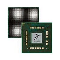
MPC8536DS Freescale Semiconductor, MPC8536DS Datasheet - Page 1235

MPC8536DS
Manufacturer Part Number
MPC8536DS
Description
BOARD DEV SYSTEM MPC8536E
Manufacturer
Freescale Semiconductor
Series
PowerQUICC III™r
Type
MPUr
Datasheets
1.MPC8536EBVTAVLA.pdf
(127 pages)
2.MPC8536EBVTAVLA.pdf
(1706 pages)
3.MPC8536DS.pdf
(2 pages)
4.MPC8536DS.pdf
(126 pages)
Specifications of MPC8536DS
Contents
Board, Software and Documentation
Processor Series
MPC85xx
Core
e500
Data Bus Width
32 bit
Maximum Clock Frequency
667 MHz
Operating Supply Voltage
- 0.3 V to + 1.21 V
Maximum Operating Temperature
+ 105 C
Data Ram Size
32 KB
Interface Type
SPI, USB
Program Memory Type
DDR2, DDR3, SDRAM
Core Size
32 Bit
Program Memory Size
544KB
Cpu Speed
1.5GHz
Digital Ic Case Style
BGA
No. Of Pins
783
Supply Voltage Range
0.95V To 1.05V
Rohs Compliant
Yes
For Use With/related Products
MPC8536
Lead Free Status / RoHS Status
Lead free / RoHS Compliant
- MPC8536EBVTAVLA PDF datasheet
- MPC8536EBVTAVLA PDF datasheet #2
- MPC8536DS PDF datasheet #3
- MPC8536DS PDF datasheet #4
- Current page: 1235 of 1706
- Download datasheet (15Mb)
19.3.2
19.3.2.1
Before queuing a command into the SATA controller, the CQR (shown in
to detect a free command queue (CQ) slot. A free CQ slot is indicated by a 0 in a bit position. To queue a
command, the bit corresponding to the CQ slot to use is set. At this point the SATA controller takes
ownership of the command header space and command descriptor associated with the command slot.
While the command is queued in the SATA controller or at the device, the command queue bit remains 1.
When the command completes, this bit is cleared to 0 by the hardware. For a device error, the CQR holds
the command queue bits at 1 for each command queued or issued to the device in error. When the host
software clears the device error, the hardware in turn clears each of the commands queued.
Freescale Semiconductor
SATA2 has the same memory-mapped registers that are described for SATA1 from 0x1_8000 to 0x1_8FFF except the
offsets are from 0x1_9000 to 0x1_9FFF.
0x40C–
0x164–
Offset
0x10C
0x14C
0x15C
0x17C
0xFFF
0x108
0x140
0x144
0x148
0x150
0x154
0x158
0x160
0x410
Command Registers
Command Queue Register (CQR)
SControl—SATA interface control register
SNotification—SATA interface notification register
TransCfg—Transport layer configuration
TransStatus—Transport layer status
LinkCfg—Link layer configuration
LinkCfg1—Link layer configuration1
LinkCfg2—Link layer configuration2
LinkStatus—Link layer status
LinkStatus1—Link layer status1
PhyCtrlCfg1—PHY control configuration1
CommandStatus—Link layer command status
Reserved
SYSPR—System priority register
Reserved
MPC8536E PowerQUICC III Integrated Processor Reference Manual, Rev. 1
Table 19-1. SATA Register Summary (continued)
Register
SATA2—Block Base Address: 0x1_9000
SATA1 System Control Registers
SATA1 Control Status Registers
Access
R/W
R/W
R/W
R/W
R/W
R/W
R/W
w1c
—
—
R
R
R
R
Figure
0x0000_FF34
0x0000_0300
0x0000_0000
0x0800_0016
0x0000_0000
0x0000_0000
0x0000_0000
0x0000_0000
0x0000_0000
0x0000_3800
0x0000_0000
0x0000_0000
Reset Value
—
—
19-2) is first examined
19.3.3.3/19-18
19.3.3.4/19-19
19.3.4.1/19-20
19.3.4.2/19-21
19.3.4.3/19-21
19.3.4.4/19-22
19.3.4.5/19-23
19.3.4.6/19-23
19.3.4.7/19-24
19.3.4.8/19-26
19.3.4.9/19-27
19.3.5.1/19-28
Section/Page
SATA Controller
—
—
19-5
Related parts for MPC8536DS
Image
Part Number
Description
Manufacturer
Datasheet
Request
R
Part Number:
Description:
Manufacturer:
Freescale Semiconductor, Inc
Datasheet:
Part Number:
Description:
Manufacturer:
Freescale Semiconductor, Inc
Datasheet:
Part Number:
Description:
Manufacturer:
Freescale Semiconductor, Inc
Datasheet:
Part Number:
Description:
Manufacturer:
Freescale Semiconductor, Inc
Datasheet:
Part Number:
Description:
Manufacturer:
Freescale Semiconductor, Inc
Datasheet:
Part Number:
Description:
Manufacturer:
Freescale Semiconductor, Inc
Datasheet:
Part Number:
Description:
Manufacturer:
Freescale Semiconductor, Inc
Datasheet:
Part Number:
Description:
Manufacturer:
Freescale Semiconductor, Inc
Datasheet:
Part Number:
Description:
Manufacturer:
Freescale Semiconductor, Inc
Datasheet:
Part Number:
Description:
Manufacturer:
Freescale Semiconductor, Inc
Datasheet:
Part Number:
Description:
Manufacturer:
Freescale Semiconductor, Inc
Datasheet:
Part Number:
Description:
Manufacturer:
Freescale Semiconductor, Inc
Datasheet:
Part Number:
Description:
Manufacturer:
Freescale Semiconductor, Inc
Datasheet:
Part Number:
Description:
Manufacturer:
Freescale Semiconductor, Inc
Datasheet:
Part Number:
Description:
Manufacturer:
Freescale Semiconductor, Inc
Datasheet:


