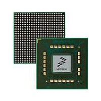
MPC8536DS Freescale Semiconductor, MPC8536DS Datasheet - Page 739

MPC8536DS
Manufacturer Part Number
MPC8536DS
Description
BOARD DEV SYSTEM MPC8536E
Manufacturer
Freescale Semiconductor
Series
PowerQUICC III™r
Type
MPUr
Datasheets
1.MPC8536EBVTAVLA.pdf
(127 pages)
2.MPC8536EBVTAVLA.pdf
(1706 pages)
3.MPC8536DS.pdf
(2 pages)
4.MPC8536DS.pdf
(126 pages)
Specifications of MPC8536DS
Contents
Board, Software and Documentation
Processor Series
MPC85xx
Core
e500
Data Bus Width
32 bit
Maximum Clock Frequency
667 MHz
Operating Supply Voltage
- 0.3 V to + 1.21 V
Maximum Operating Temperature
+ 105 C
Data Ram Size
32 KB
Interface Type
SPI, USB
Program Memory Type
DDR2, DDR3, SDRAM
Core Size
32 Bit
Program Memory Size
544KB
Cpu Speed
1.5GHz
Digital Ic Case Style
BGA
No. Of Pins
783
Supply Voltage Range
0.95V To 1.05V
Rohs Compliant
Yes
For Use With/related Products
MPC8536
Lead Free Status / RoHS Status
Lead free / RoHS Compliant
- MPC8536EBVTAVLA PDF datasheet
- MPC8536EBVTAVLA PDF datasheet #2
- MPC8536DS PDF datasheet #3
- MPC8536DS PDF datasheet #4
- Current page: 739 of 1706
- Download datasheet (15Mb)
13.5.4.4
An example of configuring FCM to execute a random page read command to large-page NAND Flash is
shown in
buffer RAM, checking ECC as it proceeds. The sequence is initiated by writing FMR[OP] = 11, and
issuing a special operation to the bank. A few cycles before completion itself, FECCn gets updated with
the ECC bytes for the main region validated by FECCn[0]. At the conclusion of the sequence, eLBC will
issue a command complete interrupt (LTESR[CC]) if interrupts are enabled. Once the sequence has
completed, the shared buffer (buffer 1 for page index 5) and transfer error registers (LTECCR that reports
the 512 blocks with unibit /multibit errors if any) are valid.
13.5.4.5
An example of configuring FCM to execute a block erase command to large-page NAND Flash is shown
in
erase status in MDR[AS0]. The sequence is initiated by writing FMR[OP] = 11, and issuing a special
Freescale Semiconductor
Table
13-48. This sequence does not require use of the shared FCM buffer RAM, but returns with the
Table
Register
FBCR
FBAR
FPAR
Register
MDR
FCR
FIR
FBCR
MDR
NAND Flash Page Read Command Sequence Example
NAND Flash Block Erase Command Sequence Example
FIR
Table 13-46. FCM Register Settings for ID Read (OR n [PGS] = 1) (continued)
13-47. This sequence reads an entire page (main and spare region) into the shared FCM
MPC8536E PowerQUICC III Integrated Processor Reference Manual, Rev. 1
Table 13-47. FCM Register Settings for Page Read (OR n [PGS] = 1)
(e.g. block 0x00010ab4)
locates page 5, buffer 1)
(e.g. 0x00005000
Initial Contents
Initial Contents
0x4125E000
0x00300000
0x00000000
0x43BBBBB0
block index
page offset
0x00000000
—
—
CMD0 = 0x00 = random read address entry;
CMD1 = 0x30 = read page
BLK locates index of 128-Kbyte block
PI locates page index in BLK;
PI mod 2 indexes FCM buffer RAM;
MS = 0 and CI = 0
BC = 0 to read entire 2112-byte page with ECC check
unused
OP0 = CM0 = command 0;
OP1 = CA = column address;
OP2 = PA = page address;
OP3 = CM1 = command 1;
OP4 = RBW = wait on Flash ready and read data into FCM buffer;
OP5–OP7 = NOP
unused
AS0 = 0x00 = dummy address for read ID command;
AS0–AS3 return with first 4 bytes of ID code
OP0 = CM0 = command 0;
OP1 = UA = user address from MDR;
OP2–OP6 = RS = read 4 bytes ID into MDR[AS3–AS0];
OP7 = NOP
Description
Description
Enhanced Local Bus Controller
13-97
Related parts for MPC8536DS
Image
Part Number
Description
Manufacturer
Datasheet
Request
R
Part Number:
Description:
Manufacturer:
Freescale Semiconductor, Inc
Datasheet:
Part Number:
Description:
Manufacturer:
Freescale Semiconductor, Inc
Datasheet:
Part Number:
Description:
Manufacturer:
Freescale Semiconductor, Inc
Datasheet:
Part Number:
Description:
Manufacturer:
Freescale Semiconductor, Inc
Datasheet:
Part Number:
Description:
Manufacturer:
Freescale Semiconductor, Inc
Datasheet:
Part Number:
Description:
Manufacturer:
Freescale Semiconductor, Inc
Datasheet:
Part Number:
Description:
Manufacturer:
Freescale Semiconductor, Inc
Datasheet:
Part Number:
Description:
Manufacturer:
Freescale Semiconductor, Inc
Datasheet:
Part Number:
Description:
Manufacturer:
Freescale Semiconductor, Inc
Datasheet:
Part Number:
Description:
Manufacturer:
Freescale Semiconductor, Inc
Datasheet:
Part Number:
Description:
Manufacturer:
Freescale Semiconductor, Inc
Datasheet:
Part Number:
Description:
Manufacturer:
Freescale Semiconductor, Inc
Datasheet:
Part Number:
Description:
Manufacturer:
Freescale Semiconductor, Inc
Datasheet:
Part Number:
Description:
Manufacturer:
Freescale Semiconductor, Inc
Datasheet:
Part Number:
Description:
Manufacturer:
Freescale Semiconductor, Inc
Datasheet:


