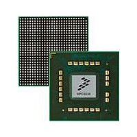
MPC8536DS Freescale Semiconductor, MPC8536DS Datasheet - Page 179

MPC8536DS
Manufacturer Part Number
MPC8536DS
Description
BOARD DEV SYSTEM MPC8536E
Manufacturer
Freescale Semiconductor
Series
PowerQUICC III™r
Type
MPUr
Datasheets
1.MPC8536EBVTAVLA.pdf
(127 pages)
2.MPC8536EBVTAVLA.pdf
(1706 pages)
3.MPC8536DS.pdf
(2 pages)
4.MPC8536DS.pdf
(126 pages)
Specifications of MPC8536DS
Contents
Board, Software and Documentation
Processor Series
MPC85xx
Core
e500
Data Bus Width
32 bit
Maximum Clock Frequency
667 MHz
Operating Supply Voltage
- 0.3 V to + 1.21 V
Maximum Operating Temperature
+ 105 C
Data Ram Size
32 KB
Interface Type
SPI, USB
Program Memory Type
DDR2, DDR3, SDRAM
Core Size
32 Bit
Program Memory Size
544KB
Cpu Speed
1.5GHz
Digital Ic Case Style
BGA
No. Of Pins
783
Supply Voltage Range
0.95V To 1.05V
Rohs Compliant
Yes
For Use With/related Products
MPC8536
Lead Free Status / RoHS Status
Lead free / RoHS Compliant
- MPC8536EBVTAVLA PDF datasheet
- MPC8536EBVTAVLA PDF datasheet #2
- MPC8536DS PDF datasheet #3
- MPC8536DS PDF datasheet #4
- Current page: 179 of 1706
- Download datasheet (15Mb)
Refer to the MPC8536E Integrated Processor Hardware Specifications for the timing requirements for
HRESET assertion and negation.
The hard reset request output signal (HRESET_REQ) indicates to external logic that a hard reset is being
requested by hardware or software. Hardware causes this signal to assert for a boot sequencer failure (see
Section 11.4.5, “Boot Sequencer
e500 watchdog timer is configured to cause a reset request when it expires. Software may request a hard
reset by setting a bit in a global utilities register; see
4.4.2
The POR sequence for the MPC8536E is as follows:
Freescale Semiconductor
1. Power is applied to meet the specifications in the MPC8536E Integrated Processor Hardware
2. The system asserts HRESET and TRST, causing all registers to be initialized to their default states
3. The system applies a stable SYSCLK signal and stable PLL configuration inputs, and the device
4. System negates HRESET after its required hold time and after POR configuration inputs have been
5. MPC8536E enables I/O drivers.
6. The MPC8536E PCI interface can assert DEVSEL in response to configuration cycles.
7. The e500 PLL configuration inputs are applied, allowing the e500 PLL to begin locking to the
8. The CCB clock is cycled for approximately 50 s to lock the e500 PLL.
9. The internal hard reset to the e500 core is negated and soft resets are negated to the PLLs and other
10. When PLL locking is completed, the local bus FCM is released provided NAND Flash is
Specifications.
and most I/O drivers to be three-stated (some clock, clock enabled, and system control signals are
active).
PLL begins locking to SYSCLK.
valid for at least 4 SYSCLK cycles.
device clock (the CCB clock).
remaining I/O blocks. The PLLs begin to lock.
configured as the boot device, as described in
FCM finishes loading the pages from the NAND Flash device, the boot sequencer, if enabled, is
allowed to progress, causing it to load configuration data from serial ROMs on the I2C1 interface,
as described in
Power-On Reset Sequence
If the JTAG signals are not used, then TRST may be tied negated. It is
recommended that TRST not remain asserted after the negation of
HRESET. TRST may be connected directly to HRESET.
There is no need to assert the SRESET signal when HRESET is asserted. If
SRESET remains asserted upon negation of HRESET, the POR sequence
will be paused after the e500 core PLL is locked and before the e500 reset
is negated. The POR sequence will be resumed when SRESET is negated.
MPC8536E PowerQUICC III Integrated Processor Reference Manual, Rev. 1
Section 11.4.5, “Boot Sequencer
Mode,” and
Section 11.4.5.2, “EEPROM Data
NOTE:
Section 23.4.1.22, “Reset Control Register
Section 4.4.3.6, “Boot ROM
Mode.”
Reset, Clocking, and Initialization
Format”) or when the
Location.” Once the
(RSTCR).”
4-9
Related parts for MPC8536DS
Image
Part Number
Description
Manufacturer
Datasheet
Request
R
Part Number:
Description:
Manufacturer:
Freescale Semiconductor, Inc
Datasheet:
Part Number:
Description:
Manufacturer:
Freescale Semiconductor, Inc
Datasheet:
Part Number:
Description:
Manufacturer:
Freescale Semiconductor, Inc
Datasheet:
Part Number:
Description:
Manufacturer:
Freescale Semiconductor, Inc
Datasheet:
Part Number:
Description:
Manufacturer:
Freescale Semiconductor, Inc
Datasheet:
Part Number:
Description:
Manufacturer:
Freescale Semiconductor, Inc
Datasheet:
Part Number:
Description:
Manufacturer:
Freescale Semiconductor, Inc
Datasheet:
Part Number:
Description:
Manufacturer:
Freescale Semiconductor, Inc
Datasheet:
Part Number:
Description:
Manufacturer:
Freescale Semiconductor, Inc
Datasheet:
Part Number:
Description:
Manufacturer:
Freescale Semiconductor, Inc
Datasheet:
Part Number:
Description:
Manufacturer:
Freescale Semiconductor, Inc
Datasheet:
Part Number:
Description:
Manufacturer:
Freescale Semiconductor, Inc
Datasheet:
Part Number:
Description:
Manufacturer:
Freescale Semiconductor, Inc
Datasheet:
Part Number:
Description:
Manufacturer:
Freescale Semiconductor, Inc
Datasheet:
Part Number:
Description:
Manufacturer:
Freescale Semiconductor, Inc
Datasheet:


