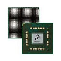
MPC8536DS Freescale Semiconductor, MPC8536DS Datasheet - Page 1695

MPC8536DS
Manufacturer Part Number
MPC8536DS
Description
BOARD DEV SYSTEM MPC8536E
Manufacturer
Freescale Semiconductor
Series
PowerQUICC III™r
Type
MPUr
Datasheets
1.MPC8536EBVTAVLA.pdf
(127 pages)
2.MPC8536EBVTAVLA.pdf
(1706 pages)
3.MPC8536DS.pdf
(2 pages)
4.MPC8536DS.pdf
(126 pages)
Specifications of MPC8536DS
Contents
Board, Software and Documentation
Processor Series
MPC85xx
Core
e500
Data Bus Width
32 bit
Maximum Clock Frequency
667 MHz
Operating Supply Voltage
- 0.3 V to + 1.21 V
Maximum Operating Temperature
+ 105 C
Data Ram Size
32 KB
Interface Type
SPI, USB
Program Memory Type
DDR2, DDR3, SDRAM
Core Size
32 Bit
Program Memory Size
544KB
Cpu Speed
1.5GHz
Digital Ic Case Style
BGA
No. Of Pins
783
Supply Voltage Range
0.95V To 1.05V
Rohs Compliant
Yes
For Use With/related Products
MPC8536
Lead Free Status / RoHS Status
Lead free / RoHS Compliant
- MPC8536EBVTAVLA PDF datasheet
- MPC8536EBVTAVLA PDF datasheet #2
- MPC8536DS PDF datasheet #3
- MPC8536DS PDF datasheet #4
- Current page: 1695 of 1706
- Download datasheet (15Mb)
Index
LA[27:31] (LBC non-multiplexed address) signals, 13-7
LAD[0:31] (LBC multiplexed address/data) signals, 13-7
LALE (LBC external address latch enable) signal, 13-5,
LBCTL (LBC data buffer control) signal, 13-7, 13-46
LBS[0:3] (LBC UPM byte select) signals, 13-6
LCK[0:2] (LBC clock) signals, 13-8
LCS[0:7] (LBC chip select) signals, 13-6
LCS[5:7] signal select
LCS0 (LBC chip select 0) signal, 13-58, 13-72
LDP[0:3] (LBC data parity) signals, 13-8
LGPL0 (LBC GP line 0) signal, 13-6
LGPL1 (LBC GP line 1) signal, 13-6
LGPL2 (LBC GP line 2) signal, 13-6
LGPL3 (LBC GP line 3) signal, 13-6
LGPL4 (LBC GP line 4) signal, 13-7
LGPL5 (LBC GP line 5) signal, 13-7
LGTA (LBC GPCM transfer acknowledge) signal, 13-7,
Little-endian, 21-6
Local access windows, 2-3–2-10
Local address map, 1-4
Local bus controller (LBC)
Freescale Semiconductor
timing, 6-27
global utilities, 23-14
ATMUs, see Address translation and mapping units
configuring local access windows, 2-8
distinguishing local access windows from other mapping
illegal interactions
L2 cache/SRAM window interactions, 2-4
precedence if overlapping among themselves, 2-8
precedence if overlapping with L2 cache/SRAM windows,
registers, 2-7–2-8
see also Local access windows, 1-4
address and address space checking, 13-43
address mask field—option registers, 13-13
atomic bus operations, 13-46
block diagram, 13-1
boot chip-select operation, 13-58, 13-72
bus monitor, 13-47
bus turnaround, 13-92
13-43
13-57
between inbound ATMUs and local access windows,
between local access windows and DDR SDRAM chip
by acronym, see Register Index
additional address phases (UPM cycles), 13-93
address following read, 13-93
read data following address, 13-93
(ATMUs)
functions, 2-9
2-4
2-10
selects, 2-9
MPC8536E PowerQUICC III Integrated Processor Reference Manual, Rev. 1
clocks and clock ratios, 13-4
configuration
debug mode
error handling
external access termination (LGTA), 13-57
features, 13-2
functional description, 13-42
general-purpose chip-select machine (GPCM), 13-48
initialization/application information, 13-90
interrupts
LCS[5:7] signal select, 23-14
memory map/register definition, 13-9
memory refresh timer prescaler, 13-23
modes of operation, 13-3
overview, 13-2
performance monitor events, 24-26
peripherals, 13-90
port sizes, 13-93
register descriptions, 13-10
signals, 13-4
UPM interfaces, 13-74–13-104
read-modify-write cycle (parity), 13-93
clock ratio register (LCRR), 13-34
LBC configuration register (LBCR), 13-32
signal selection (POR), 4-23
source and target ID, 25-4, 25-24
transfer error registers, 13-26–13-31
chip-select and write enable negation timing, 13-53
chip-select assertion timing, 13-52
extended hold time on read accesses, 13-56
GPCM mode
output enable timing, 13-56
programmable wait state configuration, 13-53
relaxed timing, 13-54
timing configuration, 13-49, 13-51, 13-68
transfer error interrupt enable register (LTEIR), 13-29
bus clock and clock ratios, 13-4
GPCM mode, registers, 13-14, 13-16
source ID debug mode, 13-4
UPM mode, registers, 13-19
GPCM timing, 13-92
hierarchy for very high speeds, 13-91
multiplexed address/data, 13-90
by acronym, see Register Index
see also Signals, LBC
block diagram, 13-75
extended hold time (reads), 13-90
programming the UPMs, 13-78
RAM array, 13-80
registers, 13-14, 13-16
address multiplexing, 13-86
byte select signal timing, 13-84
Index-9
L–L
Related parts for MPC8536DS
Image
Part Number
Description
Manufacturer
Datasheet
Request
R
Part Number:
Description:
Manufacturer:
Freescale Semiconductor, Inc
Datasheet:
Part Number:
Description:
Manufacturer:
Freescale Semiconductor, Inc
Datasheet:
Part Number:
Description:
Manufacturer:
Freescale Semiconductor, Inc
Datasheet:
Part Number:
Description:
Manufacturer:
Freescale Semiconductor, Inc
Datasheet:
Part Number:
Description:
Manufacturer:
Freescale Semiconductor, Inc
Datasheet:
Part Number:
Description:
Manufacturer:
Freescale Semiconductor, Inc
Datasheet:
Part Number:
Description:
Manufacturer:
Freescale Semiconductor, Inc
Datasheet:
Part Number:
Description:
Manufacturer:
Freescale Semiconductor, Inc
Datasheet:
Part Number:
Description:
Manufacturer:
Freescale Semiconductor, Inc
Datasheet:
Part Number:
Description:
Manufacturer:
Freescale Semiconductor, Inc
Datasheet:
Part Number:
Description:
Manufacturer:
Freescale Semiconductor, Inc
Datasheet:
Part Number:
Description:
Manufacturer:
Freescale Semiconductor, Inc
Datasheet:
Part Number:
Description:
Manufacturer:
Freescale Semiconductor, Inc
Datasheet:
Part Number:
Description:
Manufacturer:
Freescale Semiconductor, Inc
Datasheet:
Part Number:
Description:
Manufacturer:
Freescale Semiconductor, Inc
Datasheet:


