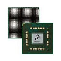
MPC8536DS Freescale Semiconductor, MPC8536DS Datasheet - Page 449

MPC8536DS
Manufacturer Part Number
MPC8536DS
Description
BOARD DEV SYSTEM MPC8536E
Manufacturer
Freescale Semiconductor
Series
PowerQUICC III™r
Type
MPUr
Datasheets
1.MPC8536EBVTAVLA.pdf
(127 pages)
2.MPC8536EBVTAVLA.pdf
(1706 pages)
3.MPC8536DS.pdf
(2 pages)
4.MPC8536DS.pdf
(126 pages)
Specifications of MPC8536DS
Contents
Board, Software and Documentation
Processor Series
MPC85xx
Core
e500
Data Bus Width
32 bit
Maximum Clock Frequency
667 MHz
Operating Supply Voltage
- 0.3 V to + 1.21 V
Maximum Operating Temperature
+ 105 C
Data Ram Size
32 KB
Interface Type
SPI, USB
Program Memory Type
DDR2, DDR3, SDRAM
Core Size
32 Bit
Program Memory Size
544KB
Cpu Speed
1.5GHz
Digital Ic Case Style
BGA
No. Of Pins
783
Supply Voltage Range
0.95V To 1.05V
Rohs Compliant
Yes
For Use With/related Products
MPC8536
Lead Free Status / RoHS Status
Lead free / RoHS Compliant
- MPC8536EBVTAVLA PDF datasheet
- MPC8536EBVTAVLA PDF datasheet #2
- MPC8536DS PDF datasheet #3
- MPC8536DS PDF datasheet #4
- Current page: 449 of 1706
- Download datasheet (15Mb)
10.3
The host processor maintains a record of current secure sessions and the corresponding keys and contexts
of those sessions. Once the host has determined that a security operation is required, it creates a
“descriptor” containing all the information the SEC needs to perform the security operation. The host
creates the descriptor in main memory, then writes a pointer to the descriptor into the fetch FIFO of one of
the SEC channels. The channel uses this pointer to read the descriptor into its descriptor buffer. Once it
obtains the descriptor, the SEC uses its bus mastering capability to obtain inputs and write results, thus
offloading data movement and encryption operations from the host processor.
Descriptors are only used in channel-controlled accesses to SEC, and not in host-controlled accesses. For
more information about host-controlled access, see
Freescale Semiconductor
1
2
Byte Address Offset
0x3_F800–0x3_FFFF
Byte accessibility is controlled by internal logic, particularly at FIFOs, to prevent unintended overwrites of partial words
during writes, and to prevent unintended duplicate reads of partial data during reads. In addition, these bytes must be
presented on the correct byte lanes for the intended destination.
For the EU FIFOs, write operations anywhere in the address range enqueue to the input FIFO, and read operations
anywhere in the address range dequeue from the output FIFO. See the referenced section for more detailed
information.
(AD 17–0)
0x3_F000
0x3_F008
0x3_F010
0x3_F018
0x3_F020
0x3_F028
0x3_F030
0x3_F038
0x3_F040
0x3_F050
0x3_F108
0x3_F400
Descriptors
MPC8536E PowerQUICC III Integrated Processor Reference Manual, Rev. 1
Module
CRCU
Table 10-3. SEC Address Map (continued)
Mode register
Key size register
Data size register
Reset control register
Control
Status register
Interrupt status register
Interrupt mask register
ICV size register
End of message register
Context register
Key register
Input FIFO
Register
Section 10.5.1.1, “Host-Controlled
Access
R/W
R/W
R/W
R/W
R/W
R/W
R/W
R/W
R/W
R/W
W
W
R
1
Write
word
word
word
word
word
word
word
word
word
byte
byte
byte
by
—
10.7.3.11/1010-106
10.7.3.12/1010-106
10.7.3.13/1010-108
10.7.3.14/1010-108
10.7.3.4/1010-100
10.7.3.5/1010-100
10.7.3.6/1010-101
10.7.3.7/1010-101
10.7.3.8/1010-102
10.7.3.9/1010-104
10.7.3.2/1010-98
10.7.3.3/1010-99
10.7.1.9/1010-67
Security Engine (SEC) 3.0
Reference
Access”.
10-19
Related parts for MPC8536DS
Image
Part Number
Description
Manufacturer
Datasheet
Request
R
Part Number:
Description:
Manufacturer:
Freescale Semiconductor, Inc
Datasheet:
Part Number:
Description:
Manufacturer:
Freescale Semiconductor, Inc
Datasheet:
Part Number:
Description:
Manufacturer:
Freescale Semiconductor, Inc
Datasheet:
Part Number:
Description:
Manufacturer:
Freescale Semiconductor, Inc
Datasheet:
Part Number:
Description:
Manufacturer:
Freescale Semiconductor, Inc
Datasheet:
Part Number:
Description:
Manufacturer:
Freescale Semiconductor, Inc
Datasheet:
Part Number:
Description:
Manufacturer:
Freescale Semiconductor, Inc
Datasheet:
Part Number:
Description:
Manufacturer:
Freescale Semiconductor, Inc
Datasheet:
Part Number:
Description:
Manufacturer:
Freescale Semiconductor, Inc
Datasheet:
Part Number:
Description:
Manufacturer:
Freescale Semiconductor, Inc
Datasheet:
Part Number:
Description:
Manufacturer:
Freescale Semiconductor, Inc
Datasheet:
Part Number:
Description:
Manufacturer:
Freescale Semiconductor, Inc
Datasheet:
Part Number:
Description:
Manufacturer:
Freescale Semiconductor, Inc
Datasheet:
Part Number:
Description:
Manufacturer:
Freescale Semiconductor, Inc
Datasheet:
Part Number:
Description:
Manufacturer:
Freescale Semiconductor, Inc
Datasheet:


