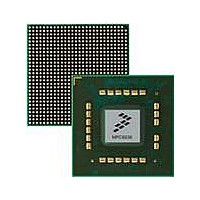
MPC8536DS Freescale Semiconductor, MPC8536DS Datasheet - Page 1585

MPC8536DS
Manufacturer Part Number
MPC8536DS
Description
BOARD DEV SYSTEM MPC8536E
Manufacturer
Freescale Semiconductor
Series
PowerQUICC III™r
Type
MPUr
Datasheets
1.MPC8536EBVTAVLA.pdf
(127 pages)
2.MPC8536EBVTAVLA.pdf
(1706 pages)
3.MPC8536DS.pdf
(2 pages)
4.MPC8536DS.pdf
(126 pages)
Specifications of MPC8536DS
Contents
Board, Software and Documentation
Processor Series
MPC85xx
Core
e500
Data Bus Width
32 bit
Maximum Clock Frequency
667 MHz
Operating Supply Voltage
- 0.3 V to + 1.21 V
Maximum Operating Temperature
+ 105 C
Data Ram Size
32 KB
Interface Type
SPI, USB
Program Memory Type
DDR2, DDR3, SDRAM
Core Size
32 Bit
Program Memory Size
544KB
Cpu Speed
1.5GHz
Digital Ic Case Style
BGA
No. Of Pins
783
Supply Voltage Range
0.95V To 1.05V
Rohs Compliant
Yes
For Use With/related Products
MPC8536
Lead Free Status / RoHS Status
Lead free / RoHS Compliant
- MPC8536EBVTAVLA PDF datasheet
- MPC8536EBVTAVLA PDF datasheet #2
- MPC8536DS PDF datasheet #3
- MPC8536DS PDF datasheet #4
- Current page: 1585 of 1706
- Download datasheet (15Mb)
25.1.2
The principal features of the debug modes and the watchpoint monitor are as follows:
25.1.3
The LBC, and DDR SDRAM interfaces all have debug modes, which are controlled by values on
configuration inputs during the power-on reset (POR) sequence, as shown in
controller can also drive debug information on either MSRCID[0:4] or MECC[0:5]. See
“Source and Target ID,”
signals in these modes.
Note that both the watchpoint monitor and trace buffer also operate in a variety of modes.
Freescale Semiconductor
Configuration
MSRCID0
MSRCID1
•
•
•
•
Signal
LBC and DDR interface source ID and data-valid indicators
— LBC or DDR SDRAM source ID can be selected to be driven onto MSRCID[0:4]
— Source ID and data-valid indicators can be selected to be driven onto the error correcting code
Watchpoint monitor that supports
— Two-level triggering
— Programmable external trigger (TRIG_OUT)
— Interlocked with performance monitor to use its large number of counters
Trace buffer features that support
— Two-level triggering
— Programmable external trigger (TRIG_OUT)
— Interlocked with performance monitor to use its large number of counters
— 256-entry trace buffer, 64 bits each
— Programmable trace start and stop
— Can function as a second watchpoint monitor
Context ID registers that can be programmed to trigger events
(ECC) pins of the DDR interface
Features
Modes of Operation
Value
POR
0
1
0
1
MPC8536E PowerQUICC III Integrated Processor Reference Manual, Rev. 1
Local bus SDRAM information appears on MSRCID[0:4] and MDVAL.
Default value (internal pull-up resistor). DDR SDRAM information appears on
MSRCID[0:4] and MDVAL.
MECC[0:4] operate in debug mode and provide memory debug source ID and
MECC5 provides data-valid information.
Default value (internal pull-up resistor). MECC[0:4] operate in normal mode and
provide DDR SDRAM error correcting code information.
Table 25-1. POR Configuration Settings and Debug Modes
for additional information about the source ID information driven on the debug
Effect
Debug Features and Watchpoint Facility
Table
25-1.The DDR
Section 25.4.1,
25.1.3.1/25-4
25.1.3.2/25-4
Reference
25-3
Related parts for MPC8536DS
Image
Part Number
Description
Manufacturer
Datasheet
Request
R
Part Number:
Description:
Manufacturer:
Freescale Semiconductor, Inc
Datasheet:
Part Number:
Description:
Manufacturer:
Freescale Semiconductor, Inc
Datasheet:
Part Number:
Description:
Manufacturer:
Freescale Semiconductor, Inc
Datasheet:
Part Number:
Description:
Manufacturer:
Freescale Semiconductor, Inc
Datasheet:
Part Number:
Description:
Manufacturer:
Freescale Semiconductor, Inc
Datasheet:
Part Number:
Description:
Manufacturer:
Freescale Semiconductor, Inc
Datasheet:
Part Number:
Description:
Manufacturer:
Freescale Semiconductor, Inc
Datasheet:
Part Number:
Description:
Manufacturer:
Freescale Semiconductor, Inc
Datasheet:
Part Number:
Description:
Manufacturer:
Freescale Semiconductor, Inc
Datasheet:
Part Number:
Description:
Manufacturer:
Freescale Semiconductor, Inc
Datasheet:
Part Number:
Description:
Manufacturer:
Freescale Semiconductor, Inc
Datasheet:
Part Number:
Description:
Manufacturer:
Freescale Semiconductor, Inc
Datasheet:
Part Number:
Description:
Manufacturer:
Freescale Semiconductor, Inc
Datasheet:
Part Number:
Description:
Manufacturer:
Freescale Semiconductor, Inc
Datasheet:
Part Number:
Description:
Manufacturer:
Freescale Semiconductor, Inc
Datasheet:


