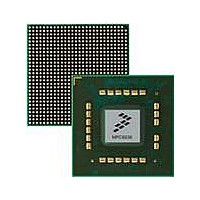
MPC8536DS Freescale Semiconductor, MPC8536DS Datasheet - Page 1271

MPC8536DS
Manufacturer Part Number
MPC8536DS
Description
BOARD DEV SYSTEM MPC8536E
Manufacturer
Freescale Semiconductor
Series
PowerQUICC III™r
Type
MPUr
Datasheets
1.MPC8536EBVTAVLA.pdf
(127 pages)
2.MPC8536EBVTAVLA.pdf
(1706 pages)
3.MPC8536DS.pdf
(2 pages)
4.MPC8536DS.pdf
(126 pages)
Specifications of MPC8536DS
Contents
Board, Software and Documentation
Processor Series
MPC85xx
Core
e500
Data Bus Width
32 bit
Maximum Clock Frequency
667 MHz
Operating Supply Voltage
- 0.3 V to + 1.21 V
Maximum Operating Temperature
+ 105 C
Data Ram Size
32 KB
Interface Type
SPI, USB
Program Memory Type
DDR2, DDR3, SDRAM
Core Size
32 Bit
Program Memory Size
544KB
Cpu Speed
1.5GHz
Digital Ic Case Style
BGA
No. Of Pins
783
Supply Voltage Range
0.95V To 1.05V
Rohs Compliant
Yes
For Use With/related Products
MPC8536
Lead Free Status / RoHS Status
Lead free / RoHS Compliant
- MPC8536EBVTAVLA PDF datasheet
- MPC8536EBVTAVLA PDF datasheet #2
- MPC8536DS PDF datasheet #3
- MPC8536DS PDF datasheet #4
- Current page: 1271 of 1706
- Download datasheet (15Mb)
19.5.1.11 BIST Support
The transmit and receive subblocks of the link layer contain logic to support BIST activate FIS
functionality.
When a BIST activate FIS is either received or transmitted successfully by the transport layer, it issues a
request to the link layer to enter BIST mode. This forces the link layer to enter a BIST state in its state
machine as soon as it receives a SYNC primitive from the far end. In the BIST state, the link layer transmits
a data sequence as specified by the two BIST data patterns in the BIST activate FIS. The link layer also
monitors the incoming data from the PHY to detect the BIST data pattern is as specified in the BIST
activate FIS. When it detects the correct data sequence, the HStatus[BIST_Err] is deasserted. The
BIST_Err bit will stay deasserted unless an error occurs in the datastream from the far end.
19.6
The PHY control layer operates between the PHY and link layers. On receive, the PHY control layer
converts the 16-bit parallel data from the PHY to a 32-bit word, which it presents to the link layer. The
PHY control layer aligns the control word of the SATA primitive to the lowest word position of the word.
The PHY control layer takes in the per-byte error signals and the per-byte control/data bits output by the
PHY and converts them into 4-bit buses, with each bit of the bus corresponding to a byte in the word.
On transmit, the PHY control layer takes in the 32-bit transmit data from the link layer and converts it to
16 bits of data which it presents to the PHY. The control/data bit from the link layer (which is always
assumed to be associated with the lowest byte position of the transmit word) is also passed onto the PHY
with the appropriate word.
19.7
19.7.1
These steps bring the SATA controller online, synchronize the SATA controller with the attached device,
and issue typical command for execution.
Freescale Semiconductor
1. Write HControl[HC_ON] = 1 to bring the SATA controller online.
2. Poll the HStatus[HS_ON] till HS_ON = 1, indicating that the controller is online.
3. Poll the SStatus[DET] till DET = 4’b0011 meaning that the device presence is detected and PHY
4. To read the device’s signature, poll HStatus[SIG_UPD] till it goes up. Read the signature from the
5. Initialize the CHBA register to point to the command header block.
6. Build a command header block in memory. Refer to
7. Build a command descriptor block in memory. Refer to
8. Build a number of PRD tables in memory as defined by the PRD_NUM field in the command
communication is established. In this state, SStatus[SPD] indicates the negotiated communication
speed.
SIG register.
header. Refer to
PHY Control Layer Overview
Initialization/Application Information
SATA Controller Initialization Steps
MPC8536E PowerQUICC III Integrated Processor Reference Manual, Rev. 1
Section 19.3.7.5, “Physical Region Descriptor Table (PRDT).”
Section 19.3.6, “Command Header.”
Section 19.3.7, “Command Descriptor.”
SATA Controller
19-41
Related parts for MPC8536DS
Image
Part Number
Description
Manufacturer
Datasheet
Request
R
Part Number:
Description:
Manufacturer:
Freescale Semiconductor, Inc
Datasheet:
Part Number:
Description:
Manufacturer:
Freescale Semiconductor, Inc
Datasheet:
Part Number:
Description:
Manufacturer:
Freescale Semiconductor, Inc
Datasheet:
Part Number:
Description:
Manufacturer:
Freescale Semiconductor, Inc
Datasheet:
Part Number:
Description:
Manufacturer:
Freescale Semiconductor, Inc
Datasheet:
Part Number:
Description:
Manufacturer:
Freescale Semiconductor, Inc
Datasheet:
Part Number:
Description:
Manufacturer:
Freescale Semiconductor, Inc
Datasheet:
Part Number:
Description:
Manufacturer:
Freescale Semiconductor, Inc
Datasheet:
Part Number:
Description:
Manufacturer:
Freescale Semiconductor, Inc
Datasheet:
Part Number:
Description:
Manufacturer:
Freescale Semiconductor, Inc
Datasheet:
Part Number:
Description:
Manufacturer:
Freescale Semiconductor, Inc
Datasheet:
Part Number:
Description:
Manufacturer:
Freescale Semiconductor, Inc
Datasheet:
Part Number:
Description:
Manufacturer:
Freescale Semiconductor, Inc
Datasheet:
Part Number:
Description:
Manufacturer:
Freescale Semiconductor, Inc
Datasheet:
Part Number:
Description:
Manufacturer:
Freescale Semiconductor, Inc
Datasheet:


