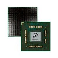
MPC8536DS Freescale Semiconductor, MPC8536DS Datasheet - Page 1096

MPC8536DS
Manufacturer Part Number
MPC8536DS
Description
BOARD DEV SYSTEM MPC8536E
Manufacturer
Freescale Semiconductor
Series
PowerQUICC III™r
Type
MPUr
Datasheets
1.MPC8536EBVTAVLA.pdf
(127 pages)
2.MPC8536EBVTAVLA.pdf
(1706 pages)
3.MPC8536DS.pdf
(2 pages)
4.MPC8536DS.pdf
(126 pages)
Specifications of MPC8536DS
Contents
Board, Software and Documentation
Processor Series
MPC85xx
Core
e500
Data Bus Width
32 bit
Maximum Clock Frequency
667 MHz
Operating Supply Voltage
- 0.3 V to + 1.21 V
Maximum Operating Temperature
+ 105 C
Data Ram Size
32 KB
Interface Type
SPI, USB
Program Memory Type
DDR2, DDR3, SDRAM
Core Size
32 Bit
Program Memory Size
544KB
Cpu Speed
1.5GHz
Digital Ic Case Style
BGA
No. Of Pins
783
Supply Voltage Range
0.95V To 1.05V
Rohs Compliant
Yes
For Use With/related Products
MPC8536
Lead Free Status / RoHS Status
Lead free / RoHS Compliant
- MPC8536EBVTAVLA PDF datasheet
- MPC8536EBVTAVLA PDF datasheet #2
- MPC8536DS PDF datasheet #3
- MPC8536DS PDF datasheet #4
- Current page: 1096 of 1706
- Download datasheet (15Mb)
PCI Bus Interface
Figure 16-64
Note that in all of these examples, the original addresses of the individual bytes within the scalars (as
created by the source) have been preserved.
16.5.2.1
All internal memory-mapped registers in the CCSR space use big endian byte ordering. However, the PCI
specification defines PCI configuration registers as little endian. All accesses to the PCI configuration port,
CFG_DATA, including the those targeting the internal PCI configuration registers, use the address
invariance policy as shown in
little-endian formatted data—either using the lwbrx/stwbrx instructions or by manipulating the data
before writing to and after reading from CFG_DATA.
16-70
Address lsbs
Significance
Byte lane
Data
Address lsbs
Significance
Byte lane
Data
Byte Order for Configuration Transactions
shows an inbound transfer of a 2-byte scalar, 0x5837, using address invariance.
PCI Configuration Space
MSB
000
54
0
MPC8536E PowerQUICC III Integrated Processor Reference Manual, Rev. 1
Figure 16-63. Address Invariant Byte Ordering—8 bytes Outbound
Figure 16-64. Address Invariant Byte Ordering—2 bytes Inbound
001
55
1
Big endian source bus
CFG_DATA
010
16
2
011
—
3
011
Figure
17
Little endian
3
source bus
010
—
Figure 16-65. CFG_DATA Byte Ordering
2
CD CE
100
4
MSB LSB
001
58
16-65. Therefore, software must access CFG_DATA with
1
Byte0
Byte3
101
MSB
5
000
37
0
110
27
6
LSB
111
28
7
Byte1
Byte2
MSB
111
28
7
MSB LSB
000
37
0
destination bus
Little endian destination bus
110
27
6
Big endian
001
58
1
101
CE CD
5
Byte2
Byte1
010
—
2
100
4
011
—
3
011
17
3
010
16
2
Freescale Semiconductor
Byte3
Byte0
LSB
001
55
1
LSB
000
54
0
Related parts for MPC8536DS
Image
Part Number
Description
Manufacturer
Datasheet
Request
R
Part Number:
Description:
Manufacturer:
Freescale Semiconductor, Inc
Datasheet:
Part Number:
Description:
Manufacturer:
Freescale Semiconductor, Inc
Datasheet:
Part Number:
Description:
Manufacturer:
Freescale Semiconductor, Inc
Datasheet:
Part Number:
Description:
Manufacturer:
Freescale Semiconductor, Inc
Datasheet:
Part Number:
Description:
Manufacturer:
Freescale Semiconductor, Inc
Datasheet:
Part Number:
Description:
Manufacturer:
Freescale Semiconductor, Inc
Datasheet:
Part Number:
Description:
Manufacturer:
Freescale Semiconductor, Inc
Datasheet:
Part Number:
Description:
Manufacturer:
Freescale Semiconductor, Inc
Datasheet:
Part Number:
Description:
Manufacturer:
Freescale Semiconductor, Inc
Datasheet:
Part Number:
Description:
Manufacturer:
Freescale Semiconductor, Inc
Datasheet:
Part Number:
Description:
Manufacturer:
Freescale Semiconductor, Inc
Datasheet:
Part Number:
Description:
Manufacturer:
Freescale Semiconductor, Inc
Datasheet:
Part Number:
Description:
Manufacturer:
Freescale Semiconductor, Inc
Datasheet:
Part Number:
Description:
Manufacturer:
Freescale Semiconductor, Inc
Datasheet:
Part Number:
Description:
Manufacturer:
Freescale Semiconductor, Inc
Datasheet:


