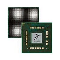
MPC8536DS Freescale Semiconductor, MPC8536DS Datasheet - Page 693

MPC8536DS
Manufacturer Part Number
MPC8536DS
Description
BOARD DEV SYSTEM MPC8536E
Manufacturer
Freescale Semiconductor
Series
PowerQUICC III™r
Type
MPUr
Datasheets
1.MPC8536EBVTAVLA.pdf
(127 pages)
2.MPC8536EBVTAVLA.pdf
(1706 pages)
3.MPC8536DS.pdf
(2 pages)
4.MPC8536DS.pdf
(126 pages)
Specifications of MPC8536DS
Contents
Board, Software and Documentation
Processor Series
MPC85xx
Core
e500
Data Bus Width
32 bit
Maximum Clock Frequency
667 MHz
Operating Supply Voltage
- 0.3 V to + 1.21 V
Maximum Operating Temperature
+ 105 C
Data Ram Size
32 KB
Interface Type
SPI, USB
Program Memory Type
DDR2, DDR3, SDRAM
Core Size
32 Bit
Program Memory Size
544KB
Cpu Speed
1.5GHz
Digital Ic Case Style
BGA
No. Of Pins
783
Supply Voltage Range
0.95V To 1.05V
Rohs Compliant
Yes
For Use With/related Products
MPC8536
Lead Free Status / RoHS Status
Lead free / RoHS Compliant
- MPC8536EBVTAVLA PDF datasheet
- MPC8536EBVTAVLA PDF datasheet #2
- MPC8536DS PDF datasheet #3
- MPC8536DS PDF datasheet #4
- Current page: 693 of 1706
- Download datasheet (15Mb)
13.4.2.2
The basic GPCM write timing parameters that may be set by the ORn attributes are shown in
The write access cycle commences upon latching of the memory address (LALE negated), and concludes
when LCSn returns high. LBCTL remains stable for the entire cycle to drive data onto any secondary data
bus. Write data becomes invalid following the falling edge of TA. LWE may, in some cases, negate high
before the end of the write access to provide additional hold time for the external memory.
Freescale Semiconductor
TRLX
Option Register Attributes
1
1
1
1
1
1
1
1
1
1
LBCTL
GPCM Write Signal Timing
LCLK
LALE
LCS n
LWE
LAD
EHTR
TA
A
0
0
0
0
1
1
1
1
1
1
MPC8536E PowerQUICC III Integrated Processor Reference Manual, Rev. 1
Notes:
t
t
t
WC
AWCS
AWE
XACS
Table 13-32. GPCM Read Control Signal Timing (continued)
= Write cycle time.
= Address valid to write enable time.
Address
0
1
1
1
0
0
0
1
1
1
= Address valid to write chip-select time.
Figure 13-37. GPCM General Write Timing Parameters
ACS
0X
0X
0X
11
10
11
10
11
10
11
t
AWCS
t
ARCS
1½
1¼
1½
t
AWE
0
2
3
0
0
2
3
1½+2×SCY
1¾+2×SCY
1½+2×SCY
2+2×SCY
1+2×SCY
1+2×SCY
2+2×SCY
2+2×SCY
1+2×SCY
1+2×SCY
Signal Timing (LCLK clock cycles)
t
Write Data
Latched Address
CSRP
t
t
t
WC
CSWP
WEN
t
CSWP
= Write enable negated time wrt chip-selec
= Write chip-select assertion period.
t
AOE
2
1
2
3
1
2
2
1
2
3
t
WEN
t
OEN
4
4
4
4
8
8
8
8
8
8
Enhanced Local Bus Controller
10+2×SCY
11+2×SCY
11+2×SCY
10+2×SCY
11+2×SCY
12+2×SCY
7+2×SCY
6+2×SCY
7+2×SCY
8+2×SCY
t
RC
Figure
13-37.
13-51
Related parts for MPC8536DS
Image
Part Number
Description
Manufacturer
Datasheet
Request
R
Part Number:
Description:
Manufacturer:
Freescale Semiconductor, Inc
Datasheet:
Part Number:
Description:
Manufacturer:
Freescale Semiconductor, Inc
Datasheet:
Part Number:
Description:
Manufacturer:
Freescale Semiconductor, Inc
Datasheet:
Part Number:
Description:
Manufacturer:
Freescale Semiconductor, Inc
Datasheet:
Part Number:
Description:
Manufacturer:
Freescale Semiconductor, Inc
Datasheet:
Part Number:
Description:
Manufacturer:
Freescale Semiconductor, Inc
Datasheet:
Part Number:
Description:
Manufacturer:
Freescale Semiconductor, Inc
Datasheet:
Part Number:
Description:
Manufacturer:
Freescale Semiconductor, Inc
Datasheet:
Part Number:
Description:
Manufacturer:
Freescale Semiconductor, Inc
Datasheet:
Part Number:
Description:
Manufacturer:
Freescale Semiconductor, Inc
Datasheet:
Part Number:
Description:
Manufacturer:
Freescale Semiconductor, Inc
Datasheet:
Part Number:
Description:
Manufacturer:
Freescale Semiconductor, Inc
Datasheet:
Part Number:
Description:
Manufacturer:
Freescale Semiconductor, Inc
Datasheet:
Part Number:
Description:
Manufacturer:
Freescale Semiconductor, Inc
Datasheet:
Part Number:
Description:
Manufacturer:
Freescale Semiconductor, Inc
Datasheet:


