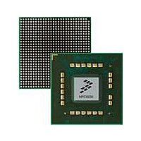
MPC8536DS Freescale Semiconductor, MPC8536DS Datasheet - Page 1587

MPC8536DS
Manufacturer Part Number
MPC8536DS
Description
BOARD DEV SYSTEM MPC8536E
Manufacturer
Freescale Semiconductor
Series
PowerQUICC III™r
Type
MPUr
Datasheets
1.MPC8536EBVTAVLA.pdf
(127 pages)
2.MPC8536EBVTAVLA.pdf
(1706 pages)
3.MPC8536DS.pdf
(2 pages)
4.MPC8536DS.pdf
(126 pages)
Specifications of MPC8536DS
Contents
Board, Software and Documentation
Processor Series
MPC85xx
Core
e500
Data Bus Width
32 bit
Maximum Clock Frequency
667 MHz
Operating Supply Voltage
- 0.3 V to + 1.21 V
Maximum Operating Temperature
+ 105 C
Data Ram Size
32 KB
Interface Type
SPI, USB
Program Memory Type
DDR2, DDR3, SDRAM
Core Size
32 Bit
Program Memory Size
544KB
Cpu Speed
1.5GHz
Digital Ic Case Style
BGA
No. Of Pins
783
Supply Voltage Range
0.95V To 1.05V
Rohs Compliant
Yes
For Use With/related Products
MPC8536
Lead Free Status / RoHS Status
Lead free / RoHS Compliant
- MPC8536EBVTAVLA PDF datasheet
- MPC8536EBVTAVLA PDF datasheet #2
- MPC8536DS PDF datasheet #3
- MPC8536DS PDF datasheet #4
- Current page: 1587 of 1706
- Download datasheet (15Mb)
25.2
This section provides information about all the external signals associated with the various MPC8536E
debug functions.
As shown in
configuration of the phase-locked loop clock mode and the ROM, flash, and dynamic memory. See
Chapter 4, “Reset, Clocking, and Initialization.”
To facilitate system testing, the MPC8536E provides a JTAG test access port (TAP) that complies with the
IEEE 1149.1 boundary-scan specification. This section also describes JTAG TAP signals.
25.2.1
All the signals associated with device debug features are summarized in
to the page number of the section with more information. The detailed descriptions are contained in
Table
described here also for completeness, with emphasis on their debugging utility.
Freescale Semiconductor
MSRCID[0:1]
MSRCID[2:4]
TRIG_OUT
MECC[0:7]
TRIG_IN
•
•
•
MDVAL
Name
TCK
25-2. Some signals (the MECC bus for example) are additionally described in other chapters, but are
Specific event selection—The trace buffer can be programmed to trace on the occurrence of one or
several concurrent events.
Specific trace selection—To facilitate trace data filtering, the trace buffer can be configured to
capture data under the following conditions:
— On every cycle in which a valid transaction is present on the selected interface
— Only when the programmed trace event is detected
Programmable trace stop—The trace buffer may be programmed to stop tracing when a
programmed stop-tracing event occurs or when the 256-entry buffer is full.
External Signal Description
Overview
Table
Description
Trigger out
DDR error
correcting
data-valid
Test clock
source ID
Trigger in
Memory
Memory
code
25-1, the MPC8536E has several signals that are sampled during POR to determine the
MPC8536E PowerQUICC III Integrated Processor Reference Manual, Rev. 1
Table 25-2. Debug, Watchpoint and Test Signal Summary
Functional
SDRAM
Debug
Debug
Debug
Debug
Debug
Block
DDR
Selectable data-valid signal from either DDR SDRAM
controller or LBC.
In debug mode, the high-order six bits carry debug
information (transaction source ID and data-valid
indication).
Selectable transaction source ID from either DDR SDRAM
controller or local bus controller.
Trigger for various function in the watchpoint monitor and
trace buffer.
Can be used externally for triggering a logic analyzer.
Additionally, it can be used for observing system ready
indication. Functions are multiplexed onto this signal
depending on TOSR[SEL] (see
Clock for JTAG testing. Internally pulled up.
Function
Table
25-25).
Table
Debug Features and Watchpoint Facility
25-2, listed with a reference
Reset_cfg O
Reset
Value
0x08
111
1
1
1
1
I/O Page #
O
O
O
O
I
I
1
25-6
25-7
25-7
25-7
25-7
25-7
25-8
25-5
Related parts for MPC8536DS
Image
Part Number
Description
Manufacturer
Datasheet
Request
R
Part Number:
Description:
Manufacturer:
Freescale Semiconductor, Inc
Datasheet:
Part Number:
Description:
Manufacturer:
Freescale Semiconductor, Inc
Datasheet:
Part Number:
Description:
Manufacturer:
Freescale Semiconductor, Inc
Datasheet:
Part Number:
Description:
Manufacturer:
Freescale Semiconductor, Inc
Datasheet:
Part Number:
Description:
Manufacturer:
Freescale Semiconductor, Inc
Datasheet:
Part Number:
Description:
Manufacturer:
Freescale Semiconductor, Inc
Datasheet:
Part Number:
Description:
Manufacturer:
Freescale Semiconductor, Inc
Datasheet:
Part Number:
Description:
Manufacturer:
Freescale Semiconductor, Inc
Datasheet:
Part Number:
Description:
Manufacturer:
Freescale Semiconductor, Inc
Datasheet:
Part Number:
Description:
Manufacturer:
Freescale Semiconductor, Inc
Datasheet:
Part Number:
Description:
Manufacturer:
Freescale Semiconductor, Inc
Datasheet:
Part Number:
Description:
Manufacturer:
Freescale Semiconductor, Inc
Datasheet:
Part Number:
Description:
Manufacturer:
Freescale Semiconductor, Inc
Datasheet:
Part Number:
Description:
Manufacturer:
Freescale Semiconductor, Inc
Datasheet:
Part Number:
Description:
Manufacturer:
Freescale Semiconductor, Inc
Datasheet:


