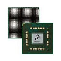
MPC8536DS Freescale Semiconductor, MPC8536DS Datasheet - Page 1617

MPC8536DS
Manufacturer Part Number
MPC8536DS
Description
BOARD DEV SYSTEM MPC8536E
Manufacturer
Freescale Semiconductor
Series
PowerQUICC III™r
Type
MPUr
Datasheets
1.MPC8536EBVTAVLA.pdf
(127 pages)
2.MPC8536EBVTAVLA.pdf
(1706 pages)
3.MPC8536DS.pdf
(2 pages)
4.MPC8536DS.pdf
(126 pages)
Specifications of MPC8536DS
Contents
Board, Software and Documentation
Processor Series
MPC85xx
Core
e500
Data Bus Width
32 bit
Maximum Clock Frequency
667 MHz
Operating Supply Voltage
- 0.3 V to + 1.21 V
Maximum Operating Temperature
+ 105 C
Data Ram Size
32 KB
Interface Type
SPI, USB
Program Memory Type
DDR2, DDR3, SDRAM
Core Size
32 Bit
Program Memory Size
544KB
Cpu Speed
1.5GHz
Digital Ic Case Style
BGA
No. Of Pins
783
Supply Voltage Range
0.95V To 1.05V
Rohs Compliant
Yes
For Use With/related Products
MPC8536
Lead Free Status / RoHS Status
Lead free / RoHS Compliant
- MPC8536EBVTAVLA PDF datasheet
- MPC8536EBVTAVLA PDF datasheet #2
- MPC8536DS PDF datasheet #3
- MPC8536DS PDF datasheet #4
- Current page: 1617 of 1706
- Download datasheet (15Mb)
A.1.5
1
A.1.6
Freescale Semiconductor
I
0x100 to 0x114.
2
C2 has the same memory-mapped registers that are described for I
0x100–
Offset
0x00C
0x000
0x004
0x008
0x010
0x014
0x114
0x500
0x500
0x500
0x501
0x501
0x502
0x502
0x502
0x503
0x504
0x505
0x506
Offset
I
DUART
2
I2CADR—I
I2CFDR—I
I2CCR—I
I2CSR—I
I2CDR—I
I2CDFSRR—I
I
URBR—ULCR[DLAB] = 0 UART0 receiver buffer register
UTHR—ULCR[DLAB] = 0 UART0 transmitter holding register
UDLB—ULCR[DLAB] = 1 UART0 divisor least significant
byte register
UIER—ULCR[DLAB] = 0 UART0 interrupt enable register
UDMB—ULCR[DLAB] = 1 UART0 divisor most significant
byte register
UIIR—ULCR[DLAB] = 0 UART0 interrupt ID register
UFCR—ULCR[DLAB] = 0 UART0 FIFO control register
UAFR—ULCR[DLAB] = 1 UART0 alternate function register
ULCR—ULCR[DLAB] = x UART0 line control register
UMCR—ULCR[DLAB] = x UART0 modem control register
ULSR—ULCR[DLAB] = x UART0 line status register
UMSR—ULCR[DLAB] = x UART0 modem status register
C Controllers
2
C2 Registers
MPC8536E PowerQUICC III Integrated Processor Reference Manual, Rev. 1
2
2
2
C status register
C control register
C data register
2
2
C frequency divider register
C address register
2
1
C digital filter sampling rate register
DUART1 & DUART2—Block Base Address 0x0_4000
I
I
2
2
C Controller 1—Block Base Address 0x0_3000
C Controller 2—Block Base Address 0x0_3100
Table A-5. I
Register
Register
Table A-6. DUARTRegisters
2
C Controller 1 & 2 Registers
UART0 Registers
I
I
2
2
C1 Registers
C2 Registers
Complete List of Configuration, Control, and Status Registers
2
C1 from 0x000 to 0x014, except the offsets range from
Access
Access
Mixed
Mixed
R/W
R/W
R/W
R/W
R/W
R/W
R/W
R/W
R/W
R/W
W
W
R
R
R
R
Reset
Reset
0x00
0x00
0x00
0x81
0x00
0x10
0x00
0x00
0x00
0x00
0x00
0x01
0x00
0x00
0x00
0x00
0x60
0x00
12.3.1.10/12-15
12.3.1.11/12-16
11.3.1.5/11-10
11.3.1.6/11-11
12.3.1.6/12-10
12.3.1.7/12-11
12.3.1.8/12-11
12.3.1.9/12-14
Section/Page
Section/Page
11.3.1.1/11-6
11.3.1.2/11-6
11.3.1.3/11-7
11.3.1.4/11-9
12.3.1.1/12-5
12.3.1.2/12-5
12.3.1.3/12-6
12.3.1.4/12-7
12.3.1.3/12-6
12.3.1.5/12-8
A-5
Related parts for MPC8536DS
Image
Part Number
Description
Manufacturer
Datasheet
Request
R
Part Number:
Description:
Manufacturer:
Freescale Semiconductor, Inc
Datasheet:
Part Number:
Description:
Manufacturer:
Freescale Semiconductor, Inc
Datasheet:
Part Number:
Description:
Manufacturer:
Freescale Semiconductor, Inc
Datasheet:
Part Number:
Description:
Manufacturer:
Freescale Semiconductor, Inc
Datasheet:
Part Number:
Description:
Manufacturer:
Freescale Semiconductor, Inc
Datasheet:
Part Number:
Description:
Manufacturer:
Freescale Semiconductor, Inc
Datasheet:
Part Number:
Description:
Manufacturer:
Freescale Semiconductor, Inc
Datasheet:
Part Number:
Description:
Manufacturer:
Freescale Semiconductor, Inc
Datasheet:
Part Number:
Description:
Manufacturer:
Freescale Semiconductor, Inc
Datasheet:
Part Number:
Description:
Manufacturer:
Freescale Semiconductor, Inc
Datasheet:
Part Number:
Description:
Manufacturer:
Freescale Semiconductor, Inc
Datasheet:
Part Number:
Description:
Manufacturer:
Freescale Semiconductor, Inc
Datasheet:
Part Number:
Description:
Manufacturer:
Freescale Semiconductor, Inc
Datasheet:
Part Number:
Description:
Manufacturer:
Freescale Semiconductor, Inc
Datasheet:
Part Number:
Description:
Manufacturer:
Freescale Semiconductor, Inc
Datasheet:


