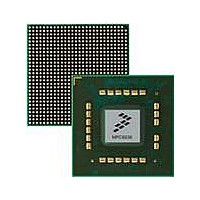
MPC8536DS Freescale Semiconductor, MPC8536DS Datasheet - Page 720

MPC8536DS
Manufacturer Part Number
MPC8536DS
Description
BOARD DEV SYSTEM MPC8536E
Manufacturer
Freescale Semiconductor
Series
PowerQUICC III™r
Type
MPUr
Datasheets
1.MPC8536EBVTAVLA.pdf
(127 pages)
2.MPC8536EBVTAVLA.pdf
(1706 pages)
3.MPC8536DS.pdf
(2 pages)
4.MPC8536DS.pdf
(126 pages)
Specifications of MPC8536DS
Contents
Board, Software and Documentation
Processor Series
MPC85xx
Core
e500
Data Bus Width
32 bit
Maximum Clock Frequency
667 MHz
Operating Supply Voltage
- 0.3 V to + 1.21 V
Maximum Operating Temperature
+ 105 C
Data Ram Size
32 KB
Interface Type
SPI, USB
Program Memory Type
DDR2, DDR3, SDRAM
Core Size
32 Bit
Program Memory Size
544KB
Cpu Speed
1.5GHz
Digital Ic Case Style
BGA
No. Of Pins
783
Supply Voltage Range
0.95V To 1.05V
Rohs Compliant
Yes
For Use With/related Products
MPC8536
Lead Free Status / RoHS Status
Lead free / RoHS Compliant
- MPC8536EBVTAVLA PDF datasheet
- MPC8536EBVTAVLA PDF datasheet #2
- MPC8536DS PDF datasheet #3
- MPC8536DS PDF datasheet #4
- Current page: 720 of 1706
- Download datasheet (15Mb)
Enhanced Local Bus Controller
timing requirements without losing data. The mechanism is the exception pattern that defines how the
UPM negates its signals in a controlled manner.
13.4.4.2
The UPM is a micro sequencer that requires microinstructions or RAM words to generate signal timings
for different memory cycles. Follow these steps to program the UPMs:
Patterns are written to the RAM array by setting MxMR[OP] = 01 and accessing the UPM with any write
transaction that hits the relevant chip select. The entire array is thus programmed by an alternating series
of writes: to MDR (RAM word to be written) each time followed by a read from MDR and then followed
by a (dummy) write transaction to the relevant UPM assigned bank. A read from MDR is required to
ensure that the MDR update has occurred prior to the (dummy) write transaction.
RAM array contents may also be read for debug purposes, for example, by alternating dummy read
transactions, each time followed by reads of MDR (when MxMR[OP] = 10).
For proper signalling, the following guidelines must be followed while programming UPM RAM words:
13-78
1. Set up BRn and ORn registers.
2. Write patterns into the RAM array.
3. Program MRTPR, LURT and MAMR[RFEN] if refresh is required.
4. Program MxMR.
•
•
•
•
For UPM reads, program UTA and LAST in the same or consecutive RAM words.
For UPM burst reads, program last UTA and LAST in the same or consecutive RAM words.
For UPM writes, program UTA and LAST in the same RAM word.
For UPM burst writes, program last UTA and LAST in the same RAM word.
Programming the UPMs
MxMR / MDR registers should not be updated while dummy read/write
access is still in progress. If the MxMR[MAD] is incremented then the
previous dummy transaction is already completed.
In order to enforce proper ordering between updates to the MxMR/MDR
register and the dummy accesses to the UPM memory region, two rules
must be followed:
1. Since the result of any update to the MxMR/MDR register must be in effect before the
2. The UPM memory region should have the same MMU settings as the memory region
dummy read or write to the UPM region, a write to MxMR/MDR should be followed
immediately by a read of MxMR/MDR.
containing the MxMR configuration register; both should be mapped by the MMU as
cache-inhibited and guarded. This prevents the CPU from re-ordering a read of the
UPM memory around the read of MxMR. Once the programming of the UPM array is
complete the MMU setting for the associated address range can be set to the proper
mode for normal operation, such as cacheable and copyback.
MPC8536E PowerQUICC III Integrated Processor Reference Manual, Rev. 1
NOTE
Freescale Semiconductor
Related parts for MPC8536DS
Image
Part Number
Description
Manufacturer
Datasheet
Request
R
Part Number:
Description:
Manufacturer:
Freescale Semiconductor, Inc
Datasheet:
Part Number:
Description:
Manufacturer:
Freescale Semiconductor, Inc
Datasheet:
Part Number:
Description:
Manufacturer:
Freescale Semiconductor, Inc
Datasheet:
Part Number:
Description:
Manufacturer:
Freescale Semiconductor, Inc
Datasheet:
Part Number:
Description:
Manufacturer:
Freescale Semiconductor, Inc
Datasheet:
Part Number:
Description:
Manufacturer:
Freescale Semiconductor, Inc
Datasheet:
Part Number:
Description:
Manufacturer:
Freescale Semiconductor, Inc
Datasheet:
Part Number:
Description:
Manufacturer:
Freescale Semiconductor, Inc
Datasheet:
Part Number:
Description:
Manufacturer:
Freescale Semiconductor, Inc
Datasheet:
Part Number:
Description:
Manufacturer:
Freescale Semiconductor, Inc
Datasheet:
Part Number:
Description:
Manufacturer:
Freescale Semiconductor, Inc
Datasheet:
Part Number:
Description:
Manufacturer:
Freescale Semiconductor, Inc
Datasheet:
Part Number:
Description:
Manufacturer:
Freescale Semiconductor, Inc
Datasheet:
Part Number:
Description:
Manufacturer:
Freescale Semiconductor, Inc
Datasheet:
Part Number:
Description:
Manufacturer:
Freescale Semiconductor, Inc
Datasheet:


