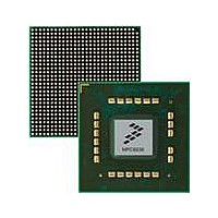
MPC8536DS Freescale Semiconductor, MPC8536DS Datasheet - Page 1199

MPC8536DS
Manufacturer Part Number
MPC8536DS
Description
BOARD DEV SYSTEM MPC8536E
Manufacturer
Freescale Semiconductor
Series
PowerQUICC III™r
Type
MPUr
Datasheets
1.MPC8536EBVTAVLA.pdf
(127 pages)
2.MPC8536EBVTAVLA.pdf
(1706 pages)
3.MPC8536DS.pdf
(2 pages)
4.MPC8536DS.pdf
(126 pages)
Specifications of MPC8536DS
Contents
Board, Software and Documentation
Processor Series
MPC85xx
Core
e500
Data Bus Width
32 bit
Maximum Clock Frequency
667 MHz
Operating Supply Voltage
- 0.3 V to + 1.21 V
Maximum Operating Temperature
+ 105 C
Data Ram Size
32 KB
Interface Type
SPI, USB
Program Memory Type
DDR2, DDR3, SDRAM
Core Size
32 Bit
Program Memory Size
544KB
Cpu Speed
1.5GHz
Digital Ic Case Style
BGA
No. Of Pins
783
Supply Voltage Range
0.95V To 1.05V
Rohs Compliant
Yes
For Use With/related Products
MPC8536
Lead Free Status / RoHS Status
Lead free / RoHS Compliant
- MPC8536EBVTAVLA PDF datasheet
- MPC8536EBVTAVLA PDF datasheet #2
- MPC8536DS PDF datasheet #3
- MPC8536DS PDF datasheet #4
- Current page: 1199 of 1706
- Download datasheet (15Mb)
17.4.1.7
As an initiator, the controller supports both type 0 and type 1 configuration cycles when configured in RC
mode. There are two methods of generating a configuration transaction; refer to
Express Configuration Space Access,”
controller’s internal configuration space, it can be sent out on the PCI Express link, or it can be internally
terminated. The PCI Express TLP header for a type 0 configuration read transaction has
TYPE[4:0] = 00100 and FMT[1] = 0; the PCI Express TLP header for a type 0 configuration write
transaction has TYPE[4:0] = 00100 and FMT[1] = 1. The PCI Express TLP header for a type 1
configuration read transaction has TYPE[4:0] = 00101 and FMT[1] = 0; the PCI Express TLP header for
a type 1 configuration write transaction has TYPE[4:0] = 00101 and FMT[1] = 1. Note that all
configuration transactions sent on PCI Express require a response regardless whether they are read or a
write configuration transactions.
The controller does not generate configuration transactions in EP mode. Only inbound configuration
transactions are supported in EP mode.
17.4.1.8
Configuration and I/O writes are serialized by the controller. The logic after issuing a configuration write
or IO write does not issue any new transactions until the outstanding configuration or I/O write is finished.
This means that an acknowledgement packet from the link partner in the form of a CpL TLP packet must
be seen or the transaction has timed out. If the CpL packet contains a CRS status, then the logic re-issues
the configuration write transaction. It keeps retrying the request until either a status other than CRS is
returned or the transaction times out.
Note that it is possible for outbound configuration read request to be requeued and be placed at the end of
the request queue due to CRS condition.
17.4.1.9
Software message generation is supported in both RC and EP modes.
17.4.1.9.1
Software can choose to send a message by programming PEXOWARn[WTT] = 0x5. A message is sent by
writing a 4-byte transaction in big-endian format that hits in an outbound window configured to send
messages.
Part of the 4-byte data is used to store information such as message code and routing information.
Table 17-121
Freescale Semiconductor
16–18
0–15
Bits
Configuration Space Addressing
Serialization of Configuration and I/O Writes
Messages
describes the message data format.
Outbound ATMU Message Generation
Routing
Name
MPC8536E PowerQUICC III Integrated Processor Reference Manual, Rev. 1
—
Table 17-121. Internal Platform (OCeaN) Message Data Format
Reset Value
—
x
for more information. A configuration transaction can hit into the
Reserved
Routing mechanism. Contains the message’s routing information
Description
PCI Express Interface Controller
Section 17.3.7, “PCI
17-103
Related parts for MPC8536DS
Image
Part Number
Description
Manufacturer
Datasheet
Request
R
Part Number:
Description:
Manufacturer:
Freescale Semiconductor, Inc
Datasheet:
Part Number:
Description:
Manufacturer:
Freescale Semiconductor, Inc
Datasheet:
Part Number:
Description:
Manufacturer:
Freescale Semiconductor, Inc
Datasheet:
Part Number:
Description:
Manufacturer:
Freescale Semiconductor, Inc
Datasheet:
Part Number:
Description:
Manufacturer:
Freescale Semiconductor, Inc
Datasheet:
Part Number:
Description:
Manufacturer:
Freescale Semiconductor, Inc
Datasheet:
Part Number:
Description:
Manufacturer:
Freescale Semiconductor, Inc
Datasheet:
Part Number:
Description:
Manufacturer:
Freescale Semiconductor, Inc
Datasheet:
Part Number:
Description:
Manufacturer:
Freescale Semiconductor, Inc
Datasheet:
Part Number:
Description:
Manufacturer:
Freescale Semiconductor, Inc
Datasheet:
Part Number:
Description:
Manufacturer:
Freescale Semiconductor, Inc
Datasheet:
Part Number:
Description:
Manufacturer:
Freescale Semiconductor, Inc
Datasheet:
Part Number:
Description:
Manufacturer:
Freescale Semiconductor, Inc
Datasheet:
Part Number:
Description:
Manufacturer:
Freescale Semiconductor, Inc
Datasheet:
Part Number:
Description:
Manufacturer:
Freescale Semiconductor, Inc
Datasheet:


