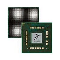
MPC8536DS Freescale Semiconductor, MPC8536DS Datasheet - Page 735

MPC8536DS
Manufacturer Part Number
MPC8536DS
Description
BOARD DEV SYSTEM MPC8536E
Manufacturer
Freescale Semiconductor
Series
PowerQUICC III™r
Type
MPUr
Datasheets
1.MPC8536EBVTAVLA.pdf
(127 pages)
2.MPC8536EBVTAVLA.pdf
(1706 pages)
3.MPC8536DS.pdf
(2 pages)
4.MPC8536DS.pdf
(126 pages)
Specifications of MPC8536DS
Contents
Board, Software and Documentation
Processor Series
MPC85xx
Core
e500
Data Bus Width
32 bit
Maximum Clock Frequency
667 MHz
Operating Supply Voltage
- 0.3 V to + 1.21 V
Maximum Operating Temperature
+ 105 C
Data Ram Size
32 KB
Interface Type
SPI, USB
Program Memory Type
DDR2, DDR3, SDRAM
Core Size
32 Bit
Program Memory Size
544KB
Cpu Speed
1.5GHz
Digital Ic Case Style
BGA
No. Of Pins
783
Supply Voltage Range
0.95V To 1.05V
Rohs Compliant
Yes
For Use With/related Products
MPC8536
Lead Free Status / RoHS Status
Lead free / RoHS Compliant
- MPC8536EBVTAVLA PDF datasheet
- MPC8536EBVTAVLA PDF datasheet #2
- MPC8536DS PDF datasheet #3
- MPC8536DS PDF datasheet #4
- Current page: 735 of 1706
- Download datasheet (15Mb)
13.5.2.1
During a read cycle, the memory/peripheral drives the bus and the bus transceiver drives LAD. After the
data has been sampled, the output drivers of the external device must be disabled. This can take some time;
for slow devices the EHTR feature of the GPCM or the programmability of the UPM should be used to
guarantee that those devices have stopped driving the bus when the eLBC memory controller ends the bus
cycle.
In this case, after the previous cycle ends, LBCTL goes high and changes the direction of the bus
transceiver. The eLBC then inserts a bus turnaround cycle to avoid contention. The external device has
now already placed its data signals in high impedance and no bus contention will occur.
13.5.2.2
During the address phase, LAD actively drives the address and LBCTL is high, driving the bus
transceivers in the same direction as during a write. After the end of the address phase, LBCTL goes low
and changes the direction of the bus transceiver. The eLBC places the LAD signals in high impedance after
its t
the transceiver starts to drive those signals after its t
ensure, that [t
13.5.2.3
Principally, a read-modify-write cycle is a read cycle immediately followed by a write cycle. Because the
write cycle will have a new address phase in any case, this basically is the same case as an address phase
after a previous read.
13.5.2.4
The flexibility of the UPM allows the user to insert additional address phases during read cycles by
changing the AMX field, therefore turning around the bus during one pattern. The eLBC automatically
inserts a single bus turnaround cycle if the bus (LAD) was previously high impedance for any reason, such
as a read, before LALE is driven and LAD is driven with the new address. The turnaround cycle is not
inserted on a write, because the bus was already driven to begin with.
However, bus contention could potentially still occur on the far side of a bus transceiver. It is the
responsibility of the designer of the UPM pattern to guarantee that enough idle cycles are inserted in the
UPM pattern to avoid this.
13.5.3
The eLBC supports 8-, 16-, and 32-bit data port sizes. However, the bus requires that the portion of the
data bus used for a transfer to or from a particular port size be fixed. A 32-bit port must reside on
LAD[0:31], a 16-bit port must reside on LAD[0:15], and an 8-bit port must reside on LAD[0:7]. The local
Freescale Semiconductor
•
•
dis
(LB). The LBCTL will have its new state after t
Write data phase after address phase
Address phase after previous write
Interface to Different Port-Size Devices
Address Phase after Previous Read
Read Data Phase after Address Phase
Read-Modify-Write Cycle for Parity Protected Memory Banks
UPM Cycles with Additional Address Phases
en
(LB) + t
MPC8536E PowerQUICC III Integrated Processor Reference Manual, Rev. 1
en
(transceiver)] is larger than t
en
(transceiver) time. The system designer has to
en
dis
(LB) and, because this is an asynchronous input,
(LB) to avoid bus contention.
Enhanced Local Bus Controller
13-93
Related parts for MPC8536DS
Image
Part Number
Description
Manufacturer
Datasheet
Request
R
Part Number:
Description:
Manufacturer:
Freescale Semiconductor, Inc
Datasheet:
Part Number:
Description:
Manufacturer:
Freescale Semiconductor, Inc
Datasheet:
Part Number:
Description:
Manufacturer:
Freescale Semiconductor, Inc
Datasheet:
Part Number:
Description:
Manufacturer:
Freescale Semiconductor, Inc
Datasheet:
Part Number:
Description:
Manufacturer:
Freescale Semiconductor, Inc
Datasheet:
Part Number:
Description:
Manufacturer:
Freescale Semiconductor, Inc
Datasheet:
Part Number:
Description:
Manufacturer:
Freescale Semiconductor, Inc
Datasheet:
Part Number:
Description:
Manufacturer:
Freescale Semiconductor, Inc
Datasheet:
Part Number:
Description:
Manufacturer:
Freescale Semiconductor, Inc
Datasheet:
Part Number:
Description:
Manufacturer:
Freescale Semiconductor, Inc
Datasheet:
Part Number:
Description:
Manufacturer:
Freescale Semiconductor, Inc
Datasheet:
Part Number:
Description:
Manufacturer:
Freescale Semiconductor, Inc
Datasheet:
Part Number:
Description:
Manufacturer:
Freescale Semiconductor, Inc
Datasheet:
Part Number:
Description:
Manufacturer:
Freescale Semiconductor, Inc
Datasheet:
Part Number:
Description:
Manufacturer:
Freescale Semiconductor, Inc
Datasheet:


