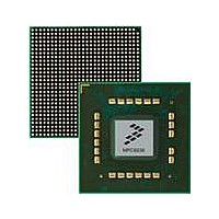
MPC8536DS Freescale Semiconductor, MPC8536DS Datasheet - Page 677

MPC8536DS
Manufacturer Part Number
MPC8536DS
Description
BOARD DEV SYSTEM MPC8536E
Manufacturer
Freescale Semiconductor
Series
PowerQUICC III™r
Type
MPUr
Datasheets
1.MPC8536EBVTAVLA.pdf
(127 pages)
2.MPC8536EBVTAVLA.pdf
(1706 pages)
3.MPC8536DS.pdf
(2 pages)
4.MPC8536DS.pdf
(126 pages)
Specifications of MPC8536DS
Contents
Board, Software and Documentation
Processor Series
MPC85xx
Core
e500
Data Bus Width
32 bit
Maximum Clock Frequency
667 MHz
Operating Supply Voltage
- 0.3 V to + 1.21 V
Maximum Operating Temperature
+ 105 C
Data Ram Size
32 KB
Interface Type
SPI, USB
Program Memory Type
DDR2, DDR3, SDRAM
Core Size
32 Bit
Program Memory Size
544KB
Cpu Speed
1.5GHz
Digital Ic Case Style
BGA
No. Of Pins
783
Supply Voltage Range
0.95V To 1.05V
Rohs Compliant
Yes
For Use With/related Products
MPC8536
Lead Free Status / RoHS Status
Lead free / RoHS Compliant
- MPC8536EBVTAVLA PDF datasheet
- MPC8536EBVTAVLA PDF datasheet #2
- MPC8536DS PDF datasheet #3
- MPC8536DS PDF datasheet #4
- Current page: 677 of 1706
- Download datasheet (15Mb)
1
Table 13-23
13.3.1.17 Flash Mode Register (FMR)
The local bus Flash mode register (FMR), shown in
Freescale Semiconductor
Offset 0x0_50E0
Reset 0
Bit R (field BOOT) is set if power-on-reset configuration selects FCM as the boot ROM target.
W
14–15
16–26
27–31
R
1–13
Bits
0
0
0 0 0 0 0 0 0 0 0 0 0 0 0 0 0
CLKDIV
describes LCRR fields.
Name
EADC
PBYP
—
—
MPC8536E PowerQUICC III Integrated Processor Reference Manual, Rev. 1
PLL bypass. This bit should be set when using low bus clock frequencies (See device hardware
specifications for applicable frequencies.). When in PLL bypass mode, incoming data is captured
in the middle of the bus clock cycle.
0 The PLL is enabled.
1 The PLL is bypassed.
Reserved
External address delay cycles of LCLK. Defines the number of cycles for the assertion of LALE.
00 4
01 1
10 2
11 3
Reserved
System clock divider. Sets the frequency ratio between the system clock and the local bus clock.
The system clock is equivalent to ccb_clk . Only the values shown below are allowed. Note that
the reset value of CLKDIV depends on the boot ROM location configuration (cfg_rom_loc[0:3]).
If the FCM is selected as the boot ROM location, the default value for CLKDIV is 0100; otherwise,
the default is 1000.
Note: It is critical that no transactions are being executed via the local bus while CLKDIV is being
00000–00001 Reserved
00010 4
00011 Reserved
00100 8 (default for boot ROM set to FCM)
00101–00111 Reserved
01000 16 (default for boot ROM not set to FCM)
01001–11111 Reserved
modified. As such, prior to modification, the user must ensure that code is not executing
out of the local bus. Once LCRR[CLKDIV] is written, the register should be read, and then
an isync should be executed.
—
Table 13-23. LCRR Field Descriptions
Figure 13-21. Flash Mode Register
15 16
0
Figure
CWTO
0
Description
0
13-21, controls global operation of the FCM.
19
0
BOOT
R
20
1
21 22
0
—
0
ECCM
23
0
Enhanced Local Bus Controller
24 25 26 27 28 29 30 31
0
—
0
0
Access: Read/Write
AL
0
0
—
0
13-35
0
OP
0
Related parts for MPC8536DS
Image
Part Number
Description
Manufacturer
Datasheet
Request
R
Part Number:
Description:
Manufacturer:
Freescale Semiconductor, Inc
Datasheet:
Part Number:
Description:
Manufacturer:
Freescale Semiconductor, Inc
Datasheet:
Part Number:
Description:
Manufacturer:
Freescale Semiconductor, Inc
Datasheet:
Part Number:
Description:
Manufacturer:
Freescale Semiconductor, Inc
Datasheet:
Part Number:
Description:
Manufacturer:
Freescale Semiconductor, Inc
Datasheet:
Part Number:
Description:
Manufacturer:
Freescale Semiconductor, Inc
Datasheet:
Part Number:
Description:
Manufacturer:
Freescale Semiconductor, Inc
Datasheet:
Part Number:
Description:
Manufacturer:
Freescale Semiconductor, Inc
Datasheet:
Part Number:
Description:
Manufacturer:
Freescale Semiconductor, Inc
Datasheet:
Part Number:
Description:
Manufacturer:
Freescale Semiconductor, Inc
Datasheet:
Part Number:
Description:
Manufacturer:
Freescale Semiconductor, Inc
Datasheet:
Part Number:
Description:
Manufacturer:
Freescale Semiconductor, Inc
Datasheet:
Part Number:
Description:
Manufacturer:
Freescale Semiconductor, Inc
Datasheet:
Part Number:
Description:
Manufacturer:
Freescale Semiconductor, Inc
Datasheet:
Part Number:
Description:
Manufacturer:
Freescale Semiconductor, Inc
Datasheet:


