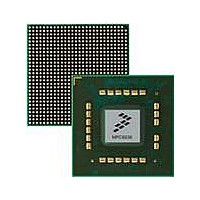
MPC8536DS Freescale Semiconductor, MPC8536DS Datasheet - Page 518

MPC8536DS
Manufacturer Part Number
MPC8536DS
Description
BOARD DEV SYSTEM MPC8536E
Manufacturer
Freescale Semiconductor
Series
PowerQUICC III™r
Type
MPUr
Datasheets
1.MPC8536EBVTAVLA.pdf
(127 pages)
2.MPC8536EBVTAVLA.pdf
(1706 pages)
3.MPC8536DS.pdf
(2 pages)
4.MPC8536DS.pdf
(126 pages)
Specifications of MPC8536DS
Contents
Board, Software and Documentation
Processor Series
MPC85xx
Core
e500
Data Bus Width
32 bit
Maximum Clock Frequency
667 MHz
Operating Supply Voltage
- 0.3 V to + 1.21 V
Maximum Operating Temperature
+ 105 C
Data Ram Size
32 KB
Interface Type
SPI, USB
Program Memory Type
DDR2, DDR3, SDRAM
Core Size
32 Bit
Program Memory Size
544KB
Cpu Speed
1.5GHz
Digital Ic Case Style
BGA
No. Of Pins
783
Supply Voltage Range
0.95V To 1.05V
Rohs Compliant
Yes
For Use With/related Products
MPC8536
Lead Free Status / RoHS Status
Lead free / RoHS Compliant
- MPC8536EBVTAVLA PDF datasheet
- MPC8536EBVTAVLA PDF datasheet #2
- MPC8536DS PDF datasheet #3
- MPC8536DS PDF datasheet #4
- Current page: 518 of 1706
- Download datasheet (15Mb)
Security Engine (SEC) 3.0
10.7.1.12.1 AESU FIFOs
AESU uses an input FIFO/output FIFO pair to hold data before and after the encryption process. Normally,
the channels control all access to these FIFOs. For host-controlled operation, a write to anywhere in the
AESU FIFO address space enqueues data to the AESU input FIFO, and a read from anywhere in the AESU
FIFO address space dequeues data from the AESU output FIFO.
Writes to the input FIFO go first to a staging register which can be written by byte, word (4 bytes), or dword
(8 bytes). When all 8 bytes of the staging register have been written, the entire dword is automatically
enqueued into the FIFO. If any byte is written twice between enqueues, it causes an error interrupt of type
AE from the EU. When writing the last portion of data, it is not necessary to write all 8 bytes. Any last
bytes remaining in the staging register are automatically padded with zeros and forced into the input FIFO
when the AESU end of message register is written.
The output FIFO is readable by byte, word, or dword. When all 8 bytes of the head dword have been read,
that dword is automatically dequeued from the FIFO so that the next dword (if any) becomes available for
reading. If any byte is read twice between dequeues, it causes an error interrupt of type AE from the EU.
Overflows and underflows caused by reading or writing the AESU FIFOs are reflected in the AESU
interrupt status register.
The AESU fetches data 128 bits at a time from the input FIFO. During processing, the input data is
encrypted or decrypted and the results are placed in the output FIFO. The output size is the same as the
input size.
The input FIFO may be written any time the number of dwords currently in the input FIFO (as indicated
by the IFL field of the AESU status register) is less than 32. There is no limit on the total number of bytes
in a message. The number of bits in the final message block must be set in the data size register.
The output FIFO may be read any time the OFR signal is asserted (as indicated in the AESU status
register). This indicates that the number of bytes in the output FIFO is at or above the threshold specified
in the mode register.
10.7.2
ARC4 Execution Unit (AFEU)
This section contains details about the ARC4 execution unit (AFEU), including modes of operation, status
and control registers, S-box memory, and FIFOs.
Most of the registers described here would not normally be accessed by the host. They are documented
here mainly for debug purposes. In typical operation, the AFEU is used through channel-controlled access,
which means that most reads and writes of AFEU registers are directed by the SEC channels. Driver
software would perform host-controlled register accesses only on a few registers for initial configuration
and error handling.
MPC8536E PowerQUICC III Integrated Processor Reference Manual, Rev. 1
10-88
Freescale Semiconductor
Related parts for MPC8536DS
Image
Part Number
Description
Manufacturer
Datasheet
Request
R
Part Number:
Description:
Manufacturer:
Freescale Semiconductor, Inc
Datasheet:
Part Number:
Description:
Manufacturer:
Freescale Semiconductor, Inc
Datasheet:
Part Number:
Description:
Manufacturer:
Freescale Semiconductor, Inc
Datasheet:
Part Number:
Description:
Manufacturer:
Freescale Semiconductor, Inc
Datasheet:
Part Number:
Description:
Manufacturer:
Freescale Semiconductor, Inc
Datasheet:
Part Number:
Description:
Manufacturer:
Freescale Semiconductor, Inc
Datasheet:
Part Number:
Description:
Manufacturer:
Freescale Semiconductor, Inc
Datasheet:
Part Number:
Description:
Manufacturer:
Freescale Semiconductor, Inc
Datasheet:
Part Number:
Description:
Manufacturer:
Freescale Semiconductor, Inc
Datasheet:
Part Number:
Description:
Manufacturer:
Freescale Semiconductor, Inc
Datasheet:
Part Number:
Description:
Manufacturer:
Freescale Semiconductor, Inc
Datasheet:
Part Number:
Description:
Manufacturer:
Freescale Semiconductor, Inc
Datasheet:
Part Number:
Description:
Manufacturer:
Freescale Semiconductor, Inc
Datasheet:
Part Number:
Description:
Manufacturer:
Freescale Semiconductor, Inc
Datasheet:
Part Number:
Description:
Manufacturer:
Freescale Semiconductor, Inc
Datasheet:


