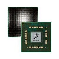
MPC8536DS Freescale Semiconductor, MPC8536DS Datasheet - Page 714

MPC8536DS
Manufacturer Part Number
MPC8536DS
Description
BOARD DEV SYSTEM MPC8536E
Manufacturer
Freescale Semiconductor
Series
PowerQUICC III™r
Type
MPUr
Datasheets
1.MPC8536EBVTAVLA.pdf
(127 pages)
2.MPC8536EBVTAVLA.pdf
(1706 pages)
3.MPC8536DS.pdf
(2 pages)
4.MPC8536DS.pdf
(126 pages)
Specifications of MPC8536DS
Contents
Board, Software and Documentation
Processor Series
MPC85xx
Core
e500
Data Bus Width
32 bit
Maximum Clock Frequency
667 MHz
Operating Supply Voltage
- 0.3 V to + 1.21 V
Maximum Operating Temperature
+ 105 C
Data Ram Size
32 KB
Interface Type
SPI, USB
Program Memory Type
DDR2, DDR3, SDRAM
Core Size
32 Bit
Program Memory Size
544KB
Cpu Speed
1.5GHz
Digital Ic Case Style
BGA
No. Of Pins
783
Supply Voltage Range
0.95V To 1.05V
Rohs Compliant
Yes
For Use With/related Products
MPC8536
Lead Free Status / RoHS Status
Lead free / RoHS Compliant
- MPC8536EBVTAVLA PDF datasheet
- MPC8536EBVTAVLA PDF datasheet #2
- MPC8536DS PDF datasheet #3
- MPC8536DS PDF datasheet #4
- Current page: 714 of 1706
- Download datasheet (15Mb)
Enhanced Local Bus Controller
13.4.3.4
Boot chip-select operation allows address decoding for a boot ROM before system initialization. LCS0 is
the boot chip-select output; its operation differs from other external chip-select outputs after a system reset.
When the core begins accessing memory after system reset, LCS0 is asserted initially to load a 4-Kbyte
boot block into the FCM buffer RAM, but core instruction fetches occur from the buffer RAM.
13.4.3.4.1
The boot chip-select also provides a programmable port size, which is configured during reset. The boot
chip-select does not provide write protection. LCS0 operates this way until the first write to OR0 and it
can be used as any other chip-select register after the preferred address range is loaded into BR0. After the
first write to OR0, the boot chip-select can be restarted only with a hardware reset.
the initial values of the boot bank in the memory controller.
13-72
FCM Boot Chip-Select Operation
FCM Bank 0 Reset Initialization
Table 13-38. Boot Bank Field Values after Reset for FCM as Boot Controller
Register
MPC8536E PowerQUICC III Integrated Processor Reference Manual, Rev. 1
BR0
LCLK
(unused)
LALE
(unused)
LCS n
LFCLE/
LFALE
LFRE
LAD[0:7]
TA
Figure 13-59. FCM Read Data Timing with Extended Hold Time
DECC
MSEL
ATOM
Field
WP
(for TRLX = 0, EHTR = 1, RST = 1, SCY = 1)
BA
PS
V
Notes:
t
t
RC
EHTR
= Read data cycle time.
read cycle
= Extended read data hold time.
last read data
t
RC
0000_0000_0000_0000_0
From cfg_rom_loc
Setting
001
00
0
0
t
EHTR
Table 13-38
Freescale Semiconductor
describes
Related parts for MPC8536DS
Image
Part Number
Description
Manufacturer
Datasheet
Request
R
Part Number:
Description:
Manufacturer:
Freescale Semiconductor, Inc
Datasheet:
Part Number:
Description:
Manufacturer:
Freescale Semiconductor, Inc
Datasheet:
Part Number:
Description:
Manufacturer:
Freescale Semiconductor, Inc
Datasheet:
Part Number:
Description:
Manufacturer:
Freescale Semiconductor, Inc
Datasheet:
Part Number:
Description:
Manufacturer:
Freescale Semiconductor, Inc
Datasheet:
Part Number:
Description:
Manufacturer:
Freescale Semiconductor, Inc
Datasheet:
Part Number:
Description:
Manufacturer:
Freescale Semiconductor, Inc
Datasheet:
Part Number:
Description:
Manufacturer:
Freescale Semiconductor, Inc
Datasheet:
Part Number:
Description:
Manufacturer:
Freescale Semiconductor, Inc
Datasheet:
Part Number:
Description:
Manufacturer:
Freescale Semiconductor, Inc
Datasheet:
Part Number:
Description:
Manufacturer:
Freescale Semiconductor, Inc
Datasheet:
Part Number:
Description:
Manufacturer:
Freescale Semiconductor, Inc
Datasheet:
Part Number:
Description:
Manufacturer:
Freescale Semiconductor, Inc
Datasheet:
Part Number:
Description:
Manufacturer:
Freescale Semiconductor, Inc
Datasheet:
Part Number:
Description:
Manufacturer:
Freescale Semiconductor, Inc
Datasheet:


