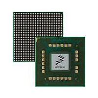
MPC8536DS Freescale Semiconductor, MPC8536DS Datasheet - Page 1123

MPC8536DS
Manufacturer Part Number
MPC8536DS
Description
BOARD DEV SYSTEM MPC8536E
Manufacturer
Freescale Semiconductor
Series
PowerQUICC III™r
Type
MPUr
Datasheets
1.MPC8536EBVTAVLA.pdf
(127 pages)
2.MPC8536EBVTAVLA.pdf
(1706 pages)
3.MPC8536DS.pdf
(2 pages)
4.MPC8536DS.pdf
(126 pages)
Specifications of MPC8536DS
Contents
Board, Software and Documentation
Processor Series
MPC85xx
Core
e500
Data Bus Width
32 bit
Maximum Clock Frequency
667 MHz
Operating Supply Voltage
- 0.3 V to + 1.21 V
Maximum Operating Temperature
+ 105 C
Data Ram Size
32 KB
Interface Type
SPI, USB
Program Memory Type
DDR2, DDR3, SDRAM
Core Size
32 Bit
Program Memory Size
544KB
Cpu Speed
1.5GHz
Digital Ic Case Style
BGA
No. Of Pins
783
Supply Voltage Range
0.95V To 1.05V
Rohs Compliant
Yes
For Use With/related Products
MPC8536
Lead Free Status / RoHS Status
Lead free / RoHS Compliant
- MPC8536EBVTAVLA PDF datasheet
- MPC8536EBVTAVLA PDF datasheet #2
- MPC8536DS PDF datasheet #3
- MPC8536DS PDF datasheet #4
- Current page: 1123 of 1706
- Download datasheet (15Mb)
17.3.5.2.4
The PCI Express inbound window base address registers, shown in
for the windows which are translated to an alternate target address space. In root complex (RC) mode,
addresses for inbound transactions are compared to these windows. In RC mode, PEXIWBAR0 is located
in the PCI Express type 1 configuration header space and PEXIWBAR[1–3] registers are implemented as
described in this section. In endpoint (EP) mode, these registers are not implemented in the
memory-mapped space. Reading these registers in EP mode returns all zeros and writing to these offsets
has no consequences. All base address registers in EP are located in the PCI Express type 0 configuration
header space. Note that PEXIWBAR1 only supports 32-bit PCI Express address space.
Table 17-20
17.3.5.2.5
The PCI Express inbound window base extended address registers, shown in
most-significant bits of a 64 bit base address.
Table 17-21
Freescale Semiconductor
Offset Window 2: 0xDCC
Reset
12–31
0–11
Bits
Offset Window 1: 0xDE8
Reset
W
R
Figure 17-22. PCI Express Inbound Window Base Extended Address Registers (PEXIWBEAR n )
W
Window 3: 0xDAC
R
0
WBEA Window base extended address. This field corresponds to PCI Express address bits [43:32]. Note that the
Name
Window 2: 0xDC8
Window 3: 0xDA8
WBA
0
Table 17-20. PCI Express Inbound Window Base Address Register Field Descriptions
Figure 17-21. PCI Express Inbound Window Base Address Registers (PEXIWBAR n )
describes the fields of the PCI Express inbound window base address registers.
describes the fields of the PCI Express inbound window base extended address registers.
PCI Express Inbound Window Base Address Registers (PEXIWBAR n )
PCI Express Inbound Window Base Extended Address Registers
(PEXIWBEAR n )
extended address is supported for windows 2 and 3 only; for PEXIWBAR1, these bits are reserved and must
be 0.
Window base address. Source address which is the starting point for the inbound translation window. The
window must be aligned based on the size selected in the window size bits. This corresponds to PCI Express
address bits [31:12].
(Windows 2 and 3 only)
MPC8536E PowerQUICC III Integrated Processor Reference Manual, Rev. 1
—
WBEA
11 12
11 12
All zeros
All zeros
Description
Figure
WBEA
WBA
17-21, select the base address
Figure
PCI Express Interface Controller
17-22, contain the
Access: Read/Write
Access: Read/Write
17-27
31
31
Related parts for MPC8536DS
Image
Part Number
Description
Manufacturer
Datasheet
Request
R
Part Number:
Description:
Manufacturer:
Freescale Semiconductor, Inc
Datasheet:
Part Number:
Description:
Manufacturer:
Freescale Semiconductor, Inc
Datasheet:
Part Number:
Description:
Manufacturer:
Freescale Semiconductor, Inc
Datasheet:
Part Number:
Description:
Manufacturer:
Freescale Semiconductor, Inc
Datasheet:
Part Number:
Description:
Manufacturer:
Freescale Semiconductor, Inc
Datasheet:
Part Number:
Description:
Manufacturer:
Freescale Semiconductor, Inc
Datasheet:
Part Number:
Description:
Manufacturer:
Freescale Semiconductor, Inc
Datasheet:
Part Number:
Description:
Manufacturer:
Freescale Semiconductor, Inc
Datasheet:
Part Number:
Description:
Manufacturer:
Freescale Semiconductor, Inc
Datasheet:
Part Number:
Description:
Manufacturer:
Freescale Semiconductor, Inc
Datasheet:
Part Number:
Description:
Manufacturer:
Freescale Semiconductor, Inc
Datasheet:
Part Number:
Description:
Manufacturer:
Freescale Semiconductor, Inc
Datasheet:
Part Number:
Description:
Manufacturer:
Freescale Semiconductor, Inc
Datasheet:
Part Number:
Description:
Manufacturer:
Freescale Semiconductor, Inc
Datasheet:
Part Number:
Description:
Manufacturer:
Freescale Semiconductor, Inc
Datasheet:


